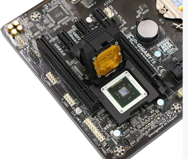
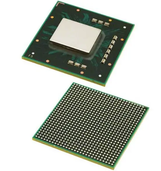
In the high-stakes world of PCB assembly, few things are as costly and frustrating as a failed Ball Grid Array (BGA). These powerful components pack immense functionality into a small footprint, but their hidden solder joints make rework difficult and expensive. Achieving a high first-pass yield (FPY) with BGAs isn't just a best practice—it's a critical metric for profitability, reliability, and time-to-market.
A low FPY means costly diagnostics, delicate rework sessions, and potential board scrap. Conversely, a high FPY signifies a robust, controlled process, resulting in reliable products and a healthy bottom line. This guide will walk you through the essential steps to consistently achieve BGA soldering perfection on the first try.
1. The Foundation: Design for Manufacturing (DFM)
Success with BGAs begins long before the assembly line. A DFM review between the designer and the manufacturer is non-negotiable.
PCB Pad Design: Follow the BGA manufacturer's recommendations exactly. Pad size is critical; it should typically be slightly smaller than the solder ball diameter (a ratio of ~0.8 is common) to ensure proper collapse and self-alignment.
Solder Mask Defined (SMD) vs. Non-Solder Mask Defined (NSMD): Prefer NSMD pads. NSMD pads, where the copper pad is smaller than the solder mask opening, provide a stronger mechanical connection to the copper trace and better solder joint reliability.
Via-in-Pad: While effective for escaping dense routing, via-in-pad must be properly filled and planarized. Unfilled vases can cause solder wicking, where solder flows down the via, starving the joint and leading to an open connection.
2. The Critical Link: Stencil Design and Solder Paste Printing
This is arguably the most influential stage. An imperfect print dooms the entire process.
Stencil Aperture Design: Do not simply match the PCB pad size. For BGA pitches above 0.5mm, a 1:1 ratio (aperture size to pad size) is often fine. For finer pitches (0.4mm and below), use a slight reduction (e.g., a 90% or 95% ratio) to prevent solder ball bridging.
Stencil Technology: For ultra-fine-pitch BGAs, consider laser-cut and electro-polished stencils. For challenging situations with mixed component types, step stencils can apply different paste volumes across the board.
Paste Inspection: Implement Automated Optical Inspection (AOI) after printing. This immediately flags boards with insufficient paste, bridging, or misalignment, allowing for cleaning and reprinting before component placement.
3. Precision Placement: Accuracy is Everything
The reflow oven is where the magic happens. A well-crafted thermal profile is vital.
Thermocouple Attachment: You cannot profile a BGA board effectively without attaching thermocouples directly to critical points. Solder one thermocouple to a thermal via under the BGA to measure the temperature at the hidden solder joints.
Key Profile Stages:
Soak/Preheat: A gradual ramp (1.0-3.0°C/second) to activate the flux and evaporate solvents. The soak should be long enough to equalize the temperature across the entire board assembly.
Reflow (Liquidus Above): The peak temperature must be high enough to fully melt the solder balls and paste, creating a new, unified solder joint. This typically requires a peak temperature of 30-40°C above the solder's melting point (e.g., 235-245°C for SAC305). Time Above Liquidus (TAL) should be held between 60-90 seconds to ensure complete reflow without over-stressing the components or board.
Ramp Rate Control: Avoid excessively fast ramp rates, which can cause thermal shock and solder splatter.
5. The Final Judge: Inspection and Quality Control
Since BGA joints are hidden, visual inspection is impossible. You must rely on technology.
Automated X-ray Inspection (AXI): This is the gold standard for BGA inspection. AXI can reveal:
Bridging: Solder shorts between adjacent balls.
Voids: Air pockets within the solder joint, which can impact thermal and mechanical performance.
Head-in-Pillow (HiP): Where the paste melts but fails to merge with the non-melting solder ball.
Cold Solder Joints: Indicated by a grainy appearance in the X-ray image.
Electrical Test: While AXI checks the physical structure, In-Circuit Test (ICT) or Flying Probe Test is essential for verifying electrical connectivity and functionality.
Conclusion: A Culture of Process Control
Achieving a high first-pass yield with BGA components is not about a single "silver bullet." It is the result of a disciplined, controlled process from design to final inspection. Each step—DFM, stencil printing, precise placement, and meticulous reflow profiling—builds upon the last.
By investing in the right tools (like AXI), rigorously applying DFM principles, and meticulously documenting and controlling your process parameters, you can transform BGA assembly from a source of anxiety into a model of reliability. The result is fewer failures, lower costs, and products that your customers can trust.