Pcb Schematic
How to Draw and Design a PCB Schematic?Contents
Guidelines to Draw a PCB Schematic DiagramOverviewA PCB schematic is the fundamental logical blueprint of an electronic circuit, marking the initial phase of product development. Adhering to established guidelines—such as precise net labeling and symbol standardization—is paramount for creating a well-organized and error-resistant design. Modern designers leverage a suite of Electronic Design Automation (EDA) tools, including Altium Designer, Cadence Allegro, Mentor Pads, KiCad, and Zuken, to generate these critical schematics. Highlights
1. Select a suitable page sizeEDA tools typically offer a range of standard page sizes. While A4 is a common default, the selection should be driven by the circuit's complexity and scale. Opt for larger formats like A3 for intricate, multi-module designs to prevent overcrowding, and smaller sizes like A5 for simple circuits. For designs targeting mass production or involving cross-team collaboration, prioritize industry-standard sizes (A4 or A3) to ensure compatibility with document management and printing systems. 2. Name the pages in alphabetical orderOrganize the schematic by dividing it into logical blocks across multiple pages. Name these pages using sequential letters (A, B, C, etc.) to establish a clear order. For instance:
3. Implement a grid system for establishing reference pointsEmploying a grid system provides essential visual reference points, aiding in the precise placement of components and wires. Always align components and connections to the grid; this practice is crucial for net probing during analysis and ensures smoother translation to PCB layout. Adopt grid spacings consistent with industry norms (e.g., 10 mil or 20 mil for general use, 5 mil for high-density designs) to maintain compatibility with EDA tool defaults and layout grids. 4. Include a title block in the footer of the pageEvery schematic page should feature a title block in its footer, containing essential metadata. This includes page size, revision, date, document number, circuit name/function, project name/number, author, reviewer, approver, company name, and relevant standards (e.g., IEEE 315). For regulated industries, extend the title block to include compliance certifications (e.g., ISO 26262 ASIL level, IEC 60601-1 edition) and traceability codes linked to requirement documents. What is the importance of a schematic diagram?The schematic diagram is a cornerstone of electronic design. A well-crafted schematic clearly visualizes the electrical connections between components and the circuit's intended functionality, serving as the primary communication tool for designers, reviewers, and manufacturers. Beyond technical correctness, clarity is vital; a congested schematic can be misleading and hinder troubleshooting. Furthermore, a detailed and compliant schematic is indispensable for adhering to industry standards, reducing production errors, enabling effective collaboration, and supporting regulatory audits. 5. Add important notes/comments on separate pagesCritical design instructions and constraints should be documented as notes. For complex designs, dedicate a separate page for these comments. Examples include:
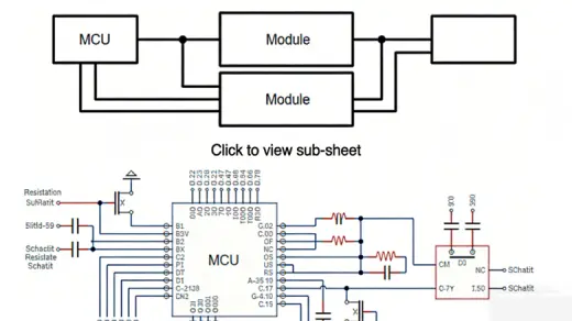
6. Include a revision history on the first or last pageMaintain a revision history log, typically on the first or last page, to track all design changes. Each entry should include the revision version (e.g., A0, A1, B0), date, description of changes, names of the author and reviewer, and approval status. Implement a clear versioning scheme: use "A0" for initial release, "A1" for minor updates (typos, formatting), and "B0" for major changes (component swaps, functional modifications). For audits, retain a complete record including change justification and stakeholder sign-off. 7. Incorporate a table of contents into the schematic documentFor multi-page, complex designs, a table of contents greatly enhances navigability. It should list page numbers, module names, and key components (e.g., "Page C: MCU Interface - U1 (STM32F407), U2 (ETH PHY)"). In collaborative environments, adding a column for "Design Owner" can clarify responsibilities. This page can be omitted for simple, single-page schematics. 8. Utilize a block diagram to illustrate design modules and the signal flowA block diagram provides a high-level overview of the system's major functional modules and their interconnections. It is an invaluable tool for reviewers and new team members to grasp the overall design architecture quickly. For complex systems, label each block with its function, key ICs, and signal types. In hierarchical designs, hyperlink blocks to their corresponding detailed schematic pages.
9. Illustrate the signal flow path using a hierarchical schematic designFor sophisticated designs with numerous sub-circuits, a hierarchical schematic structure is recommended. This approach clearly depicts signal flow between top-level modules (like a block diagram) while allowing drill-down into detailed circuit pages for each module. Maintain consistent signal flow direction (e.g., inputs on left, outputs on right) across all levels. Clearly define inter-module interfaces (e.g., "Power_Enable: from Controller to Regulator") at the top level. 10. Employ standard component reference designatorsAssign component designators according to recognized standards like IEEE 315-2009, using uppercase letters. This ensures universal understanding. For large projects, number components sequentially within each module (e.g., power supply resistors R1-R10, MCU section resistors R11-R20) to aid identification.
11. Generate component symbols using the standard library
The schematic diagram consists of different types of components, such as active components, passive components, and connectors. Active components include transistors, diodes, logic gates, processor IC, FPGA, Op-amps, and so on. Components like capacitors, inductors, and transformers are referred to as passive devices. Creating new symbols is not advisable unless the symbol for that component is not present in the standard library (compliant with IEEE 315-2009, IEC 60617, or ANSI Y32.2). For custom symbols, document the design rules, pin mappings, and compliance checks (e.g., cross-referenced with manufacturer datasheet) and store them in a certified company library with version control.
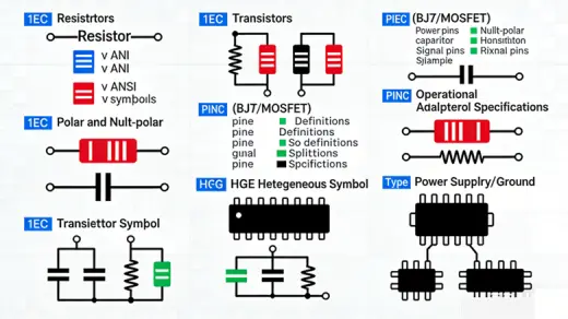
ResistorsResistors can be represented in two different ways. You should take care to keep up the consistency in the symbols used. The unit of the resistance is ohms and is represented by the symbol 'Ω.' Sometimes, the symbol 'Ω' can be replaced with the letter 'E'. You should ensure that consistent unit representation is followed throughout the entire design. All required data about the components should be entered in the design tool (e.g., resistance value, tolerance, power rating, package size, MPN). This makes it easier to create a BOM at the end of the design. For high-power resistors (≥1W), add thermal dissipation notes in the schematic (e.g., "R5: 2W, heatsink required").
Polarized and non-polarized capacitorsCapacitors have two terminals, one positive and one negative. Care should be taken to mark the polarity of these terminals. An error in the polarity of the capacitor terminal might lead to exploding. The capacitor symbols should follow IEEE 315-2009 standards. You should also ensure that the pin numbers assigned to the symbols match the footprint layout. For decoupling capacitors, annotate the associated IC and power rail (e.g., "C10: VCC_3.3V Decoupling for U1 (STM32)"). For high-frequency applications (≥1MHz), specify the capacitor type (e.g., "C12: 0.1μF X7R Ceramic") in the schematic or BOM to ensure performance.
TransistorsA transistor is a three-terminal semiconductor device. The terminals are the base, collector, and emitter (BJT) or gate, source, drain (MOSFET). You should always refer to the component datasheet while mapping the pins in the footprint layout to the schematic symbol. When the symbols are created, it is important to enter a description of the component (e.g., "Q3: NPN BJT, 2N3904, Ic=200mA"). This is very useful for future reference or when the part is obsolete and needs to be replaced. Having these details on the BOM improves readability. For power transistors, add thermal management notes (e.g., "Q8: MOSFET, IRF540N, heatsink required") and current rating annotations (e.g., "Id=33A").
Op-amp
It is very important to create the op-amp symbol per the IEEE 315-2009 standards. Many designers often draw the op-amp as per their convenience, which tends to lose readability. When you create a symbol, it is recommended to have all the input pins on the left and all the output pins on the right. Similarly, power and ground pins can be placed at the top and bottom, respectively. You should be careful while flipping or changing the orientation of the symbol. Failure to adjust the wiring after flipping symbols can lead to misalignments between the schematic and physical connections, potentially causing incorrect functionality or circuit failure. Hence, care should be taken to cross-check each symbol with the manufacturer's datasheet. For precision op-amps, annotate offset voltage, bandwidth, and power supply requirements (e.g., "U4: Op-amp, AD8605, Vcc=±5V, Vos=1μV") in the schematic or BOM.
Heterogeneous schematic symbolComplex devices such as FPGA, memory, and microprocessors are called heterogeneous components. These components have different types of pins in large numbers, such as data lines, inputs/outputs, address lines, control lines, and power lines. To retain clarity and readability, you should create multiple components of a single package, such as UxA, UxB, UxC, and UxD. Some pins on components may have multiple functions, and this flexibility is usually denoted on the symbol, accompanied by specific details provided outside the symbol. For FPGAs or microprocessors, group pins by function (e.g., UxA: Power/Ground, UxB: Digital I/O, UxC: Analog Inputs) and include a cross-reference table linking pin numbers to datasheet pinout for verification.
Power and ground symbolsIt is always a good idea to represent voltages with a '+' sign since there could be negative voltages present on the board. You should follow a standard and consistent convention to represent the voltage levels and their sections inside the silicon (e.g., +3.3V_IO, +3.3V_DG, +3.3V_AN, +1.8V_Core, +1.2V_LVCore, +2.5_Vref). Similarly, different types of grounds could be present on the board (e.g., GND_DIGITAL, GND_ANALOG, GND_POWER, GND_SHIELD), and their symbols must comply with IEEE 315-2009. Clearly separate analog and digital grounds in the schematic to avoid crosstalk, and annotate ground plane separation requirements (e.g., "Analog-Digital Ground: Isolate with 2mm gap in layout"). For high-voltage designs (≥50V), use distinct power symbols (e.g., HV_+120V) and add safety warnings (e.g., "High Voltage: Risk of Electric Shock").
12. Reduce unnecessary net connections to enhance clarityWhenever you have two wires that form a junction and share an electrical connection, that intersection needs to have a junction dot. This is a standard practice in every schematic design. However, most schematic design software applications exclude the junction dot when a wire connects directly to a pin or terminal on a component.
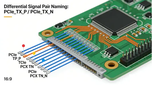
Net labeling conventionsThe objective of a schematic is to make your circuitry easier to understand for you as a designer. Unnecessary net connections should be minimized. Rather than drawing dozens of nets all over the place, you can assign a net name for a specific pin, which is associated with a pin on another device. These pins will have the same name. Pins with the same name are assumed to be connected. This improves the readability of a schematic. This approach is especially beneficial when the net is linked to three or more locations. For differential signals, use industry-standard naming conventions (e.g., DDR4_DQ0_P/DDR4_DQ0_N, PCIe_TX_P/PCIe_TX_N) to indicate paired signals. For clock signals, append frequency information (e.g., CLK_16MHz) to avoid ambiguity.
Net labeling guidelinesWhen nets are connected on the same page directly to another IC, net naming is not
required. You can follow these simple rules while naming the nets: · Signal names should always be written in uppercase and should be placed just above the net. · Avoid long names. Preferably, the names can have a maximum of 8 characters (extended from 4 to balance clarity and brevity) while retaining key information (e.g., 3.3V_IO instead of VCC). · Describe active low or high signals using the upper bar (e.g., $\overline{RESET}$ for active low reset) or suffix (e.g., RESET_N) – choose one convention and apply it consistently. · Open nets/connections should be removed. · For critical signals (reset, clock, power rails), add priority labels (e.g., "PRIO_HIGH") to guide layout engineers. · For nets requiring length matching (e.g., DDR data lines), annotate the target length (e.g., "LEN_MATCH: 50mm ±0.5mm") and group name (e.g., "DDR4_DQ_GROUP1").
Off-page connectionTo improve readability, designers usually name the nets in the schematic. This works fine when the signal is to be connected on the same page. If there is a requirement to connect the net to a pin that is present on a different page, an off-page connector symbol should be used. Label off-page connectors with the target page number and net name (e.g., "PAGE_C: I2C_SDA") for traceability. For multi-board designs, add board identification (e.g., "BOARD2_PAGE_D: SPI_CLK") to avoid cross-board connection errors. Ensure that off-page connectors are consistently styled (per IEEE 315) and listed in the table of contents for easy reference.
Signal flow representationOn a schematic page, the signal flows from the left to right side of the page. Any power and ground connections are shown on the top or bottom side of the page, respectively. You are advised to keep this in mind and to keep components accordingly. For power distribution networks (PDN), represent the flow from primary power (e.g., 12V_IN) to regulators (e.g., LDO_3.3V) to load ICs (e.g., U1_STM32) in a top-to-bottom hierarchy. For analog circuits, separate signal paths (input→amplifier→filter→output) clearly and annotate signal types (e.g., "ANALOG_IN: 0-5V") to avoid confusion with digital signals.
13. Maintain readability when depicting the component placementComponent placement in a schematic is one of the important tasks. This is because the layout engineer is going to keep the components accordingly. Group related components (e.g., a voltage regulator, input capacitor, output capacitor) in close proximity on the schematic to reflect their physical placement. Avoid crossing signal lines whenever possible; use net labels instead of direct wires for long connections. For dense modules, use color coding (per company standards) to distinguish signal types (e.g., red for power, blue for digital I/O, green for analog) – ensure colorblind accessibility (e.g., use patterns in addition to color).
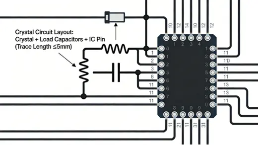
14. Place components connected to the crystal in close proximityCrystal placement in the schematic should group related high-frequency components close together. Typically, when the design requires placing two components in close proximity, they should be illustrated accordingly (e.g., shunt and series terminations). For high-frequency crystals (≥10MHz), annotate load capacitance requirements (e.g., "Crystal: 24MHz, CL=18pF") and keep the crystal, load capacitors, and IC oscillator pins within a 1cm radius on the schematic (to guide layout). Add notes to avoid trace stubs and minimize parasitic capacitance in the crystal circuit (e.g., "No vias under crystal; keep traces short (<5mm)").
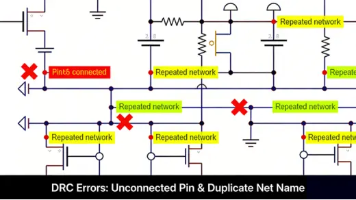
15. Run a DRC to assess the integrity of the designDesign Rule Check (DRC) is an intelligent feature offered by CAD software to check both the logical and physical integrity of a design. Checks are made against all enabled design rules and can be made online as you design. Configure DRC rules to comply with industry standards and project requirements: · Logical rules: Unconnected pins, duplicate net names, incorrect component symbols, polarity errors. · Physical rules (schematic-driven layout): Component footprint compatibility, net length constraints, impedance requirements. · Industry-specific rules: EMC (e.g., IEC 61000-4-2), safety (e.g., IEC 60950-1 creepage/clearance). Run DRC at key milestones (after module completion, before netlist export) and document all violations and resolutions (e.g., "DRC Violation: Unconnected pin U1_Pin12 → Resolved: Connected to GND_ANALOG").
16. Manually verify the nets to eliminate potential design errorsThe netlist is generated when the schematic design is complete and ready to be imported into the layout. The most common file extension for netlist is the .net. Manually verifying the nets is recommended to avoid design errors. Perform a netlist cross-check with the schematic to ensure: · All components are included with correct reference designators and footprints. · Net connections match the schematic (no missing or extra connections). · Power and ground nets are correctly assigned (e.g., +3.3V_IO connected to all I/O pins, GND_ANALOG isolated from GND_DIGITAL). · For high-speed signals, verify differential pair integrity (e.g., no unpaired differential nets, correct polarity). Use a "netlist walkthrough" with the design team to validate critical paths (e.g., reset, clock, power).
17. Generate complete BOM by importing components from the libraryCurrently, CAD tools provide a key feature called BOM creation. A complete and sufficient BOM can be generated only if you have provided all the inputs in the tools while creating or importing components from the library. The inputs to the BOM could be MPN (Manufacturing Part Number), package, vendor name, vendor part number, quantity, component value, tolerance, power rating, compliance certifications (RoHS 3, REACH, IATF 16949), lifecycle status (active/obsolete), and alternative MPNs. It is recommended to provide all the required information during the symbol creation. For regulated industries: · Automotive: Include IATF 16949 vendor certification, AEC-Q qualification (e.g., AEC-Q100 for ICs). · Medical: Add ISO 13485 compliance, biocompatibility ratings (if applicable). · Aerospace: Include MIL-SPEC part numbers and radiation tolerance (e.g., MIL-PRF-55355). Export the BOM in industry-standard formats (CSV, XML, IPC-2581) for compatibility with procurement and manufacturing systems.
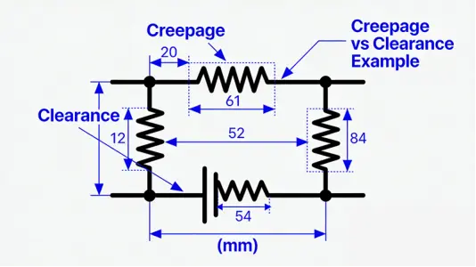
18. Comply with industry-specific standards and normsAlign the schematic with international and industry-specific standards to ensure compliance, interoperability, and safety: Core standards· IEEE 315-2009: Component symbol standard (pinout, symbol shapes, labeling). · IEC 60617: Graphical symbols for electrical and electronic diagrams (global harmonization). · IPC-2221: Generic standard for printed board design (schematic-to-layout translation). · ANSI Y32.2: American standard for electrical symbols (for North American markets). Industry-specific standards· Automotive: ISO 26262 (functional safety) – annotate safety mechanisms (e.g., watchdog, redundant sensors), ASIL level for critical modules, and fault mode analysis (FMEA) references. · Medical: IEC 60601-1 (safety of medical electrical equipment) – label isolated circuits (e.g., "Galvanic Isolation: 5kV"), creepage/clearance requirements, and patient-connected components. · Industrial: IEC 61508 (functional safety) – document safety integrity level (SIL) for control circuits, redundancy design, and diagnostic coverage. · Aerospace: MIL-STD-883 (microcircuits) – use MIL-qualified components, annotate radiation hardening, and comply with DO-254 for avionics. Standard updatesUpdate standards regularly: Track revisions (e.g., IEEE 315-2009 vs. draft revisions) and adapt symbols/labeling to reflect changes (e.g., new symbols for USB4, PCIe 6.0).
19. Adapt to special scenario requirements
High-speed/high-frequency circuits (≥100MHz or DDR, PCIe, Ethernet)Schematic constraints: · Differential pairs: Label with "_P/_N" suffix, annotate impedance (e.g., 100Ω for PCIe), and specify length matching (e.g., ±0.1mm for DDR5). · Termination: Include series resistors (R_S) for transmission lines, parallel resistors (R_T) for open-ended nets, and annotate values (e.g., "R_T: 50Ω for 1Gbps Ethernet"). · Clock signals: Isolate clock paths from noisy nets, add ferrite beads for EMI suppression, and annotate jitter requirements (e.g., "CLK_JITTER: <10ps RMS"). EMC considerations: · Filter capacitors: Place near IC power pins (annotate "0.1μF X7R, ≤5mm from VCC pin") to suppress switching noise. · Grounding: Use separate analog/digital/power grounds, annotate star grounding or ground plane split requirements. Shielding: Label shielded connectors (e.g., "J3: Shielded USB-C") and annotate shield grounding (e.g., "Shield connected to GND_SHIELD at
· single point"). Power integrity (PI) optimizationPower rail design: · Annotate voltage ripple limits (e.g., "3.3V_IO: Ripple <50mVpp"). · Include power tree hierarchy (e.g., "12V_IN → LDO1 → 3.3V_Core → U1_STM32"). · Add decoupling capacitor arrays for high-current ICs (e.g., "U2_FPGA: 4x 0.1μF + 1x 10μF decoupling"). Thermal management: · Annotate power dissipation for high-power components (e.g., "U3_LDO: 2W, heatsink required"). · Label thermal vias in the schematic (e.g., "Thermal vias under Q6: 4x 0.3mm") to guide layout. Low-power designs· Annotate sleep/wake-up signals (e.g., "SLEEP_EN: Active low, current <1μA in sleep mode"). · Label power gating circuits (e.g., "PG_3.3V: Turn off when not in use") and low-power component ratings (e.g., "U4: 1μA quiescent current").
20. Standardize collaboration and compliance documentation
Version management· Follow strict revision control: Use "A0" (initial) → "A1" (minor) → "B0" (major) → "B1" (minor) naming. · Document revision types: Minor (format, typo), Major (component/function change), Critical (safety/compliance fix). · Link revisions to requirements: Include change request (CR) numbers, user stories, or regulatory updates (e.g., "Revision B0: CR-2024-003 – Update to RoHS 3"). Collaboration workflows· Peer review (PR) process: Define review checklists (e.g., symbol compliance, net labeling, safety annotations), assign reviewers by expertise (e.g., EMC engineer for high-frequency modules), and document comments/resolutions. · Cross-team coordination: Label module ownership (e.g., "Power Module: Electrical Team; MCU Module: Firmware Team") and interface specifications (e.g., "I2C Interface: SDA/SCL, 100kHz, Pull-up 4.7kΩ"). · Tool compatibility: Use industry-standard EDA tool formats (e.g., Altium .SchDoc, KiCad .kicad_sch) and export schematics as PDF/A (archival format) for long-term storage.
Compliance documentation· Regulatory traceability: Link schematic elements to compliance requirements (e.g., "C12: RoHS 3 compliant – Ref: REACH Annex XVII"). · Intellectual property (IP): Annotate open-source symbols (e.g., "Symbol from KiCad Library: CC BY-SA 4.0") and company-owned custom symbols (e.g., "Proprietary Symbol – Confidential"). · Audit trails: Retain records of all revisions, reviews, and approvals (electronic signatures for regulated industries) for regulatory audits (e.g., FDA for medical devices, EPA for environmental compliance).
21. Refine component and network design details
Component-symbol-footprint consistency· Ensure schematic symbols match the manufacturer’s datasheet (pin numbering, polarity, pin functions) and footprint (package type, pin spacing). · Annotate footprint details in the schematic (e.g., "R1: 0402, 1206 for power resistors") to avoid layout mismatches. · For custom footprints, link to footprint documentation (e.g., "Footprint: Custom_QFP100 – Ref: FP-2024-001") and verify with IPC-7351 (land pattern standard). Special component annotations· ESD protection: Label ESD diodes (e.g., "D5: ESD Protection, ±8kV contact discharge per IEC 61000-4-2") and their placement (e.g., "Near J1_USB-C"). Fuses: Include rating (current, voltage, speed) and type (e.g., "F1: 1A
· Fast-Acting, 250V, Surface Mount"). · Connectors: Annotate pin definitions (e.g., "J2_Pin1: VCC_5V, Pin2: GND, Pin3: UART_TX") and keying features (e.g., "J2: Keyed connector – No reverse insertion"). Network design refinements· Redundant/spare nets: Label spare pins (e.g., "GPIO_RESERVED") and redundant paths (e.g., "Redundant Power Path: U5_LDO → U1_STM32_VCC") for future upgrades. · Test points: Add test point symbols for critical nets (e.g., "TP1: 3.3V_Core, TP2: CLK_16MHz") with labels and pad size (e.g., "TP_PAD: 1.2mm") to facilitate manufacturing testing. · Signal priority: Classify signals as high/medium/low priority (e.g., "PRIO_HIGH: Reset, Clock; PRIO_MED: Data Lines; PRIO_LOW: Status LEDs") to guide layout resource allocation.
22. Standardize EDA tool operations and verification processesEDA tool configuration· Library management: Use certified, version-controlled libraries (compliant with IEEE 315) and avoid unvetted third-party libraries. Implement library validation checks (e.g., symbol-footprint matching, compliance with standards) before use. · Default settings: Configure tool grids (10mil), net labeling conventions, and DRC rules to align with company/industry standards. Save configuration profiles for reuse across projects. · Data exchange: Export schematics/netlists in industry-standard formats: o Netlist: IPC-D-356 (standard netlist format for PCB manufacturing). o BOM: IPC-2581 (integrated BOM, schematic, and layout data). o Documentation: PDF/A (archival), SVG (vector graphics for reports). Verification process· Schematic-layout cross-verification: After layout completion, compare the layout netlist with the schematic netlist to ensure no unintended changes (e.g., missing connections, incorrect component placement). · DFM (Design for Manufacturing) checks in schematic: o Annotate component accessibility (e.g., "Q7: Place for hand soldering – No under-component vias"). o Label solder mask openings (e.g., "TP1: Solder mask open for test probe access"). · Simulation integration: For critical circuits (e.g., power regulators, analog amplifiers), link the schematic to SPICE simulation tools (e.g., PSpice, LTspice) and document simulation results (e.g., "Voltage regulation: ±2% tolerance verified via simulation").
23. Add safety design and troubleshooting auxiliary specificationsSafety design annotations· High-voltage/hazardous signals: Label high-voltage areas (e.g., "HV_ZONE: 120VAC – Danger: Electric Shock") with standardized warning symbols (per IEC 60417). · Overcurrent/overvoltage protection: Annotate protection circuits (e.g., "F1 + D1: Overcurrent/Overvoltage Protection for 5V Rail") and their trip points (e.g., "F1: Trip at 2A"). · Fire safety: Use flame-retardant component ratings (e.g., "Capacitors: UL94 V-0") and annotate in the schematic. Troubleshooting aids· Test points: As noted earlier, add test points for key nets (power rails, clock signals, data lines) with clear labels and locations. · Diagnostic signals: Include test pins for internal diagnostics (e.g., "DIAG_OK: High when system is operational") and annotate their function. · Schematic cross-references: Link components to datasheets (e.g., "U1: STM32F407 – Datasheet: DS100000001") and add notes for common troubleshooting scenarios (e.g., "If U1 does not power on: Check C10 (decoupling capacitor) and F1 (fuse)").
The schematic checklist is the most often ignored point in schematic creation. This is more related to the organization's process, which is based on past design experiences. Having a checklist avoids errors in the schematic and makes the design robust. Below is the expanded checklist: 1. Verify pin numbering and labels for each component and align them according to the datasheet. 2. Conduct a polarity check for all polarized components (capacitors, diodes, transistors) in the schematic. 3. Check for overlapping labels and pin numbers to ensure legibility. 4. Validate the alignment of the base, collector, and emitter (BJT) or gate, source, drain (MOSFET) pins of transistors with the datasheet, schematic symbol, and footprint package. 5. Confirm the accuracy of component values, reference designators, and physical locations. 6. Ensure the presence of schematic symbol descriptions, such as MPN, vendor name, vendor part number, compliance certifications, and lifecycle status. 7. Check for the presence and accuracy of off-page connectors, including target page/board labels. 8. Verify inter-sheet references for seamless connectivity. 9. Conduct checks on decoupling capacitors for all ICs, ensuring proper ground pin separation based on signal type (analog, digital, signal, ground). 10. Perform bill of materials checks, including package types, quantity, part numbers, compliance, and alternative parts. 11. Validate compliance with industry-specific standards (IEEE 315, ISO 26262, IEC 60601, etc.). 12. Verify high-speed/high-frequency design constraints (differential pairs, impedance, length matching). 13. Check EMC and PI-related annotations (filter capacitors, grounding, shielding). 14. Confirm revision history completeness (date, author, reviewer, change description, associated CRs). 15. Validate DRC results and resolution of all violations. 16. Verify netlist accuracy (no missing/extra connections, correct power/ground assignment). 17. Check safety annotations (high-voltage labels, creepage/clearance, protection circuits). 18. Confirm test point placement and labeling for manufacturing/troubleshooting. Validate collaboration documentation (peer review comments, module
1. ownership, interface specs). 2. Ensure compatibility with EDA tool formats and data exchange standards (IPC-D-356, IPC-2581).
ConclusionSchematic is the backbone of any circuit board design. A good schematic should ensure a seamless transition from a good concept to a layout. From net labeling to component symbol creation, from industry compliance to special scenario adaptation, you need to adhere to the set of standard guidelines to ensure an error-free, compliant, and manufacturable PCB schematic. Need assistance in creating schematics for your design? Post your queries on PCBMO; our design experts will help you!
|