PCB DESIGN
|
Professional PCB Design: Comprehensive Solutions for High-Performance Electronic ProductsWhat is PCB Design?1. Introduction to PCB Design1.1 Definition of PCB DesignPCB design is a technical process that translates customer functional requirements into practical electronic circuit layouts. It encompasses creating PCB schematics, optimizing the placement of electronic components, arranging circuit connections, and integrating considerations such as electromagnetic compatibility (EMC), heat dissipation, and manufacturability. Beyond mere circuit drawing, excellent PCB design aims to balance performance enhancement, cost control, and debugging convenience, laying a solid foundation for the production of high-quality electronic products. 1.2 Core Significance of PCB DesignHigh-quality PCB design is crucial for electronic products. It not only reduces PCB manufacturing costs by optimizing material usage and production processes but also significantly improves product performance—enhancing signal integrity, reducing electromagnetic interference (EMI), and ensuring stable operation under various working conditions. For enterprises, efficient PCB design shortens product development cycles, enabling faster market entry and gaining a competitive edge in industries such as network communication, industrial control, and automotive electronics. 1.3 Key Application Fields of PCB DesignPCB design has a wide range of applications across multiple high-tech industries, including:
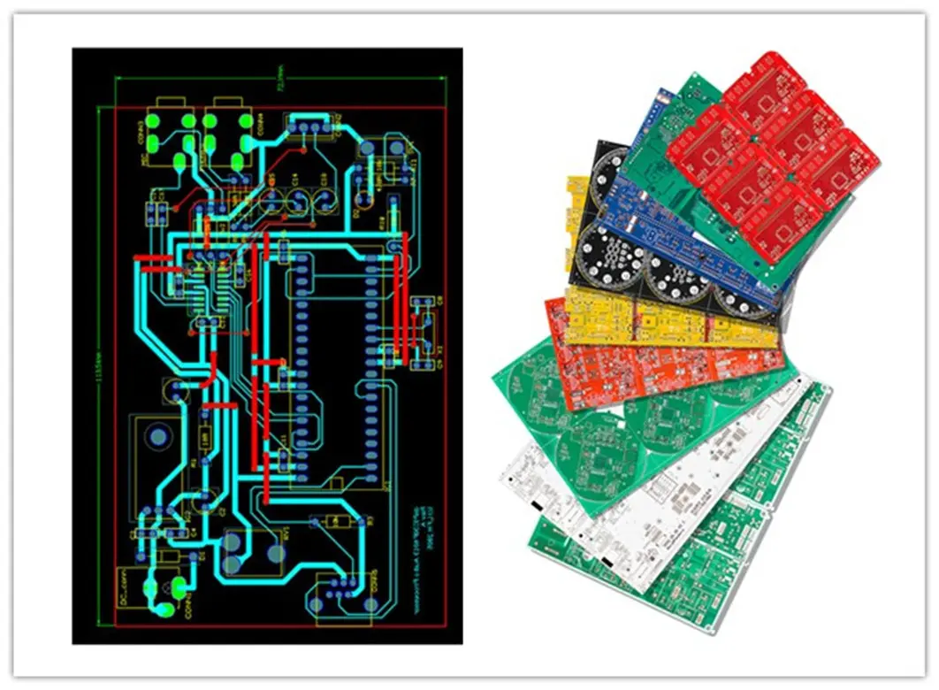
2. Core Foundation of PCB Design2.1 Essential Concepts and Terminology2.1.1 PCB SchematicThe PCB schematic is a graphical representation of the circuit's functional structure, depicting the electrical connections between components. It serves as the blueprint for PCB design, guiding subsequent layout and wiring work. Creating accurate and standardized schematics is critical to ensuring the circuit's functionality. 2.1.2 PCB LayoutPCB layout refers to the physical placement of electronic components on the circuit board and the routing of copper traces to realize electrical connections. A rational layout optimizes signal transmission paths, minimizes interference, and facilitates manufacturing and assembly. It is a core link that directly affects product performance. 2.1.3 Multilayer PCB DesignMultilayer PCB design involves using circuit boards with multiple conductive layers (up to 42 layers in advanced designs) to meet the requirements of high-density, high-performance electronic products. This design reduces board size, shortens signal paths, and improves signal integrity, making it widely used in complex devices such as servers and aerospace equipment. 2.1.4 PCB Prototype DesignPCB prototype design is the process of creating small-batch sample boards before mass production. It verifies the feasibility of the design, identifies potential issues in advance, and provides a basis for design optimization. Rapid prototype production (with delivery in as little as 48 hours) accelerates product development cycles. 2.2 Preparatory Work for PCB Design2.2.1 Establishment of Component Libraries
2.2.2 Schematic Design and Network Table GenerationUse professional PCB schematic design tools to draw schematics according to product functions, then generate corresponding network tables. For simple circuits, manual network table generation and component packaging placement are feasible, but consistency between schematic pin names and packaging library names (especially for diodes and triodes) must be ensured. 3. Technical Specializations in PCB Design3.1 High-Speed PCB Design and Signal Integrity3.1.1 Key Requirements for High-Speed PCB DesignHigh-speed PCB design (supporting signals up to 60GHz) requires precise control of signal transmission speed, impedance matching, and crosstalk. It involves optimizing trace routing, selecting appropriate materials, and designing reasonable ground planes to ensure signal integrity—avoiding signal distortion or delay. 3.1.2 Signal Integrity Simulation & AnalysisConduct signal integrity simulations to predict and resolve potential issues such as reflection, crosstalk, and electromagnetic interference. By analyzing signal waveforms and transmission characteristics, designers optimize the layout and wiring to improve the circuit's stability and reliability. 3.1.3 Impedance Matching and Differential Pair Routing
3.2 Special Processes and Structural Design3.2.1 HDI PCB DesignHDI (High-Density Interconnect) PCB design features small line widths (minimum 2.4mil), narrow line spacing (minimum 2.4mil), and high pin density (up to 110,000+ pins). It uses microvias and blind/buried vias to achieve high-density interconnections, suitable for compact, high-performance products like mobile phones and medical devices. 3.2.2 Flexible and Rigid-Flex PCB Design
3.2.3 High-Frequency and RF PCB DesignHigh-frequency PCB design (for applications like C/Ku band tuners) and RF (Radio Frequency) PCB design require specialized materials and layout techniques to reduce signal loss and electromagnetic interference. Key considerations include controlled impedance, shielding design, and optimized component placement. 3.3 Design for Manufacturability (DFM), Testability (DFT), and Assembly (DFA)3.3.1 Design for Manufacturability (DFM)Incorporate manufacturing requirements into the design phase, considering factors such as PCB size, trace width, via size, and component spacing. This minimizes production defects, reduces costs, and improves production efficiency. 3.3.2 Design for Testability (DFT)Add test points and test circuits to the design to facilitate post-production testing, enabling rapid detection of faults and ensuring product quality. 3.3.3 Design for Assembly (DFA)Optimize component placement and layout to simplify the SMT (Surface Mount Technology) assembly process, reduce assembly time and errors, and improve production yield. 4. PCB Design Process and Stages4.1 Four Core Stages of PCB Design
4.2 Key Links in the Design Process4.2.1 PCB Structure DesignBased on the circuit board size and mechanical positioning requirements, draw the PCB frame in the design environment, and place connectors, buttons, screw holes, and assembly holes. Clearly define wiring and non-wiring areas (e.g., areas around screw holes) to ensure structural rationality. 4.2.2 Component Layout1.Prioritize the placement of key components (core chips, high-voltage components, high-heat components, and easily interfered components) to ensure circuit functionality and signal integrity. 4.2.3 Wiring DesignFollow design rules such as minimum line width and spacing, optimize trace routing to shorten signal paths, reduce crosstalk and interference, and ensure stable electrical connections. For high-speed and high-frequency circuits, use specialized wiring techniques (e.g., differential pair routing). 4.2.4 Design Review and Optimization1.Self-Inspection: Check layout, wiring, design rules, aesthetics, and thermal design structure. 4.3 Post-Design Processes: Prototype and Assembly4.3.1 PCB Prototype FabricationProduce small-batch prototypes based on the design documents to verify design feasibility and performance. Professional manufacturing teams ensure prototype quality and rapid delivery. 4.3.2 PCB Assembly (PCBA)Combine prototype boards with electronic components (via machine or hand placement) to form finished PCBA boards. Full inspection is standard, with additional tests available upon request. 4.3.3 Testing and OptimizationBurn firmware into PCBA boards for functional testing, performance optimization, and problem troubleshooting. Component procurement, replacement of compatible components, and design of test racks are also included in this phase. 5. PCB Design Software and Tools5.1 Commonly Used PCB Design Software1.Altium Series (Protel, Altium Designer): Widely used in China, featuring a user-friendly interface and simple operation, suitable for general PCB design but less ideal for complex projects. 5.2 Selection of PCB Design Tools1.Beginners: Cadence SPB is recommended to develop good design habits. 5.3 Auxiliary Tools and Resources1.PCB Design Calculators: Used for calculating impedance, trace width, via size, and other parameters. 6. Industry-Specific PCB Design Solutions1.Automotive PCB Design: Requires high reliability, temperature resistance, and anti-interference capabilities, focusing on power integrity and EMC compliance. 7. PCB Design Services and Advantages of PCBmo7.1 Comprehensive Service Scope1.Custom PCB Design Service: Tailor solutions from initial concepts or schematics, offering one-stop services including manufacturing, assembly, and testing. 7.2 Core Advantages of PCBmo's PCB Design Services1.Professional Team with Rich Experience: Senior team with over 15 years of experience, completing 2000+ PCB design projects annually. 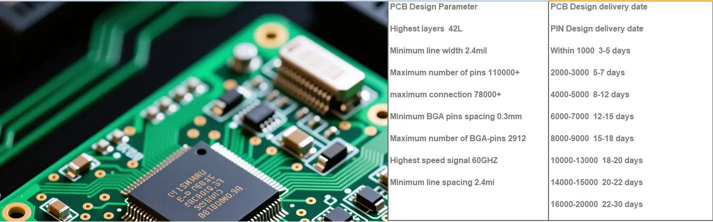
5.High-Standard Confidentiality Measures: Signed confidentiality agreements and fully encrypted designer computers. 8. Common Problems and Solutions in PCB Design8.1 PCB Design Mistakes to Avoid1.Inconsistent component library pin definitions. 8.2 Solutions to Common Technical IssuesSignal Interference1.Separate analog and digital circuits. Heat Dissipation Problems1.Place high-heat components in well-ventilated areas. Manufacturability Issues1.Strictly follow DFM rules. 8.3 FAQ on PCB Design1.How to Design a PCB? Follow the four core stages: refine concept, conduct feasibility study, design hardware/software, and perform testing. 9. Conclusion and Call to Action9.1 Summary of PCB Design ValuePCB design is a core link in electronic product development, integrating technology, experience, and innovation. It ensures product performance, reduces costs, and shortens time-to-market. 9.2 PCBmo's Commitment and Services
As a professional PCB and PCBA manufacturing company, PCBmo provides one-stop services from PCB design, manufacturing, and assembly to testing. We are committed to delivering high-quality, cost-effective solutions for customers worldwide. 9.3 Call to ActionIf you have PCB design needs—whether custom services, turnkey solutions, or industry-specific designs—please contact PCBmo. We offer professional technical support, timely consultation, and flexible cooperation models to help you turn ideas into high-performance products. Let us work together to achieve success in the competitive electronic product market.
|