PCB Stencil: The Cornerstone of High-Quality SMT Assembly
Key Takeaways
-
A PCB stencil is a critical tool for SMT assembly, enabling precise, consistent solder paste deposition that directly impacts solder joint quality and product reliability.
-
Stencil manufacturing methods (laser cutting, electroforming, chemical etching) vary in precision, cost, and speed—laser cutting is the most versatile for high-precision applications.
-
The application process (design, alignment, printing, inspection, cleaning) requires strict adherence to specifications to avoid defects like bridging and weak solder joints.
-
Framed, frameless, and step stencils each serve distinct production needs, with framed stencils ideal for high-volume, complex PCBs and frameless stencils suited for low-volume, flexible production.
-
Choosing the right stencil involves balancing PCB design, component requirements, production volume, and budget—prioritizing precision for fine-pitch components and durability for high-volume runs.
What Is a PCB Stencil and Its Role in SMT Assembly?
In the realm of electronic manufacturing, Surface Mount Technology (SMT) has become the backbone of assembling compact, high-performance printed circuit boards (PCBs). At the heart of this technology lies the PCB stencil, a precision tool that dictates the accuracy, consistency, and reliability of solder paste application—directly influencing the functionality and performance of the final electronic product.
Without a well-designed and properly used PCB stencil, achieving defect-free SMT assembly becomes a daunting task, leading to increased risks of solder bridging, tombstoning, and weak solder joints. This comprehensive guide delves into every aspect of PCB stencils, from their definition and manufacturing to their application, types, advantages, challenges, and selection criteria.
What is a PCB Stencil?
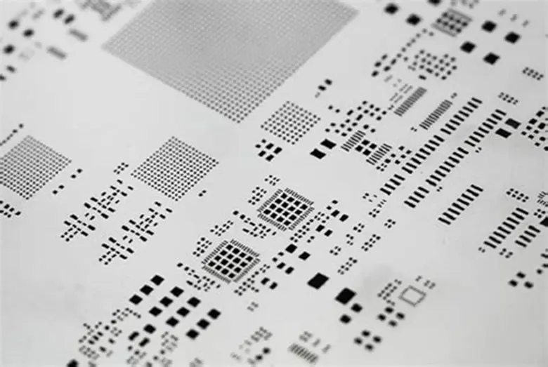
A PCB stencil, also known as an SMT stencil or circuit board stencil, is a thin sheet of material—most commonly stainless steel or nickel—featuring precisely laser-cut, chemically etched, or electroformed apertures. These apertures are strategically aligned to match the location of SMT component pads on a bare PCB.
The primary function of the stencil is to deposit the exact amount of solder paste onto designated pads, ensuring that when SMT components are placed and subjected to reflow soldering, the resulting solder joints are mechanically robust and electrically conductive.
PCB stencils are available in a range of thicknesses, typically between 0.05mm and 0.2mm:
-
Thicker stencils offer greater durability, making them suitable for high-volume production runs.
-
Thinner stencils provide the flexibility needed for intricate PCB designs with micro-pitch components like Ball Grid Arrays (BGAs) and Quad Flat No-leads (QFNs) .
The precision of the stencil’s apertures is paramount—laser-cut and electroformed stencils, for instance, boast an opening accuracy of ±5~25μm, enabling consistent solder paste deposition even for the smallest components.
PCB Stencil Manufacturing Process
The manufacturing of a PCB stencil is a precision-driven process that directly impacts its performance. Stencils are categorized based on their aperture formation methods, with three primary techniques dominating the industry:
1. Laser Cutting (Subtractive Process)
Laser cutting is the most widely used method for producing high-precision stencils.
-
Process: Uses a computational CNC laser cutter driven by the PCB’s Gerber data to remove unwanted material from a stainless steel foil.
-
Accuracy: Creates apertures with a tolerance of ±0.05mm—regardless of the aperture size.
-
Key Advantage: Ability to create trapezoidal (rather than vertical) openings, which facilitates efficient solder paste release and reduces the risk of paste sticking to aperture walls.
-
Considerations: Delivers consistent, high-quality results and is cost-effective for fine-pitch components, but manufacturing speed is relatively slower compared to other methods.
2. Electroforming (Additive Process)
Electroforming is an additive process that builds up the stencil by electroplating nickel around a photo-resist template of the desired apertures.
-
Key Advantage: Excels at creating small apertures with ultra-fine pitches, as the resulting aperture walls are smooth and mirror-like—promoting optimal solder paste release.
-
Cost Note: The cost is independent of the number of apertures, making it ideal for stencils with a high density of openings.
-
Considerations: Has a long processing time and high initial manufacturing costs.
3. Chemical Etching (Subtractive Process)
Chemical etching uses acid to dissolve material from a metal sheet, forming apertures.
-
Advantages: Low-cost, high-speed method suitable for large openings.
-
Disadvantages: Produces rough aperture sidewalls and often results in an "hourglass" shape for the holes, making it unsuitable for fine-pitch components as it increases the risk of solder defects like bridging.
In addition to aperture formation, stencil manufacturing may include a polishing process to enhance performance. Common polishing methods include mechanical polishing (simple and cost-effective but time-consuming), chemical polishing (highly precise but requiring careful handling), and electropolishing (delivers a smooth finish but requires specialized equipment and is expensive).
PCB Stencil Application Process
The effective use of a PCB stencil involves a structured, multi-step process that ensures accurate solder paste deposition and consistent assembly results.
1. Design Phase
The design phase is critical to stencil performance.
-
Aperture Design: Tailored to the PCB’s pad type (square, round, oval) and component requirements. For precision components like BGAs and QFNs, chamfered designs (e.g., rounded aperture corners) are used to prevent solder paste from pulling at the component tips.
-
Aperture Size: Typically 5%~10% smaller than the corresponding PCB pads (e.g., a 1.0mm pad uses a 0.95mm aperture) to avoid solder paste overflow and bridging.
-
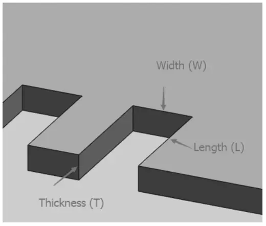
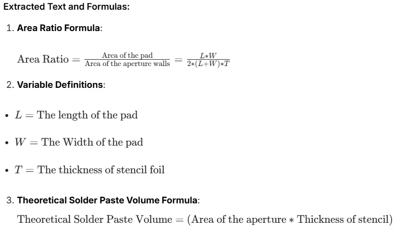
Key Ratios:
2. Installation and Alignment
Proper alignment between the stencil and PCB is essential for accurate paste deposition.
-
Fixing: Stencils are fixed to the printing machine platform using clamps or magnetic frames.
-
Mechanical Alignment: Locating pins (Fiducial Pins) align with the PCB’s reference holes.
-
Optical Alignment: Optical cameras identify fiducial marks on both the PCB and stencil to automatically compensate for any offsets.
3. Solder Paste Printing
-
Paste Preparation: Before printing, solder paste is stirred for 2-3 minutes to restore its viscosity and rheology.
-
Squeegee Types:
-
Squeegee Angle: Angled at 15-20 degrees toward the direction of movement, with light to medium constant pressure applied to ensure the stencil contacts the PCB surface and solder paste is forced through the apertures.
4. Detection and Correction
After printing, Solder Paste Inspection (SPI) systems use laser or structured light scanning to measure the height, volume, and area of the deposited solder paste. Data from the SPI is linked to the printer, which automatically adjusts squeegee pressure or stencil position to correct deviations. Manual inspection—using magnifying glasses or microscopes—checks for uniformity, bridging, or contamination.
5. Cleaning and Maintenance
Regular cleaning prevents aperture clogging, which can cause solder defects.
-
Dry Cleaning: Uses a vacuum nozzle to remove residual solder paste from the stencil surface.
-
Deep Cleaning: Involves spraying a cleaning agent (e.g., alcohol or deionized water) and ultrasonic oscillation (40kHz) to clear debris from the apertures.
-
Lifespan: Proper maintenance extends the stencil’s lifespan—stainless steel stencils, for example, can be reused thousands of times under normal conditions.
Types of PCB Stencils
PCB stencils are classified based on their mounting style and design features, each suited to specific production needs:
1. Framed PCB Stencils
Framed stencils consist of a stencil foil mounted on a mesh, which is then attached to an aluminum frame. The frame provides tension to the stencil, ensuring it remains flat during printing.
-
Advantages: Enhanced accuracy and consistency, durability, and compatibility with automated pick-and-place machines.
-
Disadvantages: Higher upfront costs, require more storage and transportation space, and offer limited flexibility for adjustments.
-
Best For: Large, complex PCBs and high-volume production.
2. Frameless PCB Stencils
Frameless stencils are stored as flat foils and fitted into a reusable frame for use. This design allows multiple stencils to be used with a single frame.
-
Advantages: Cost-effective, flexible for adjustments, and reduces storage requirements—four times as many frameless stencils can be stored in the same space as framed ones.
-
Disadvantages: Reduced durability and a higher risk of misalignment during printing.
-
Best For: Low-volume production or quick changeovers between different PCBs.
3. Step Stencils
Step stencils feature apertures of different sizes on multiple levels, enabling precise deposition of varying amounts of solder paste on different areas of the PCB.
-
Advantages: Ideal for PCBs with mixed component sizes and pitches, reduces waste, and ensures optimal solder joints for each component type.
-
Disadvantages: Higher manufacturing costs and longer production times; less compatible with automated machines.
-
Best For: PCBs requiring varying solder paste volumes for different components.
4. Hybrid PCB Stencils
Hybrid stencils combine features of different types (e.g., laser-cut apertures for fine-pitch components and chemically etched apertures for larger pads) to balance performance and cost. They are tailored to specific PCB designs that require a mix of precision and affordability.
Advantages and Disadvantages of PCB Stencils
Advantages
-
High Precision and Consistency: Laser-cut and electroformed stencils deliver aperture accuracy of ±5~25μm, supporting micro-pitch components. Aperture design controls solder paste volume, reducing defects like cold solder joints and bridging.
-
High Production Efficiency: Automated printers complete a single print in 3-10 seconds, making stencils ideal for mass production. Integration with SPI systems and pick-and-place machines enables full-process automation.
-
Adaptability to Complex Designs: Stencils support specialized features like anti-tin bead grooves and local thickening (step stencils), meeting the needs of high-density PCBs and irregularly shaped pads.
-
Reusability: Stainless steel stencils have a long lifespan, with thousands of reuses possible under proper maintenance, reducing long-term production costs.
Disadvantages
-
High Initial Cost: High-precision stencils (e.g., laser-cut or electroformed) can cost $100-500 per piece, depending on the manufacturer, making them a significant upfront investment.
-
Complex Maintenance: High-density PCBs require frequent stencil cleaning (e.g., every 50 prints) to prevent aperture clogging, adding to production time and labor costs.
-
Environmental Sensitivity: High temperatures or mechanical stress can reduce stencil tension, compromising printing accuracy.
-
Limitations in Special Scenarios: For flexible PCBs (FPCs), aligning the stencil with the flexible substrate is challenging, leading to potential offsets.
Key Factors for Choosing the Right PCB Stencil
Selecting the optimal PCB stencil requires careful consideration of the following factors:
-
PCB Size and Complexity: Larger, more complex PCBs benefit from framed stencils, which provide stable support and alignment. Smaller, simpler PCBs can use frameless stencils to reduce costs and storage needs.
-
Aperture Design and Size: Aperture dimensions must match the PCB’s pad size and component requirements. Fine-pitch components require laser-cut or electroformed apertures, while larger pads may use chemically etched apertures. The 5%~10% reduction in aperture size relative to pads prevents solder overflow.
-
Material and Construction: Stainless steel is the most common stencil material, offering durability and corrosion resistance. Nickel is lighter and more flexible, suitable for harsh environments but more expensive. Electroformed stencils are the most precise and durable.
-
Solder Paste Type: Solder paste viscosity and particle size influence stencil performance. For example, high-viscosity paste may require larger apertures or metal squeegees to ensure proper deposition.
-
Production Volume: High-volume production benefits from framed stencils, which support automated processes and long-term use. Low-volume production or prototyping can use frameless stencils to minimize costs.
-
Framework Material: Stencil frameworks are typically made of stainless steel (durable but heavy), nickel (lightweight but expensive), or aluminum (cost-effective but less durable). The choice depends on handling requirements, environmental conditions, and budget.
Formula to Calculate the Approximate Thickness of the PCB Stencil
The image includes a formula for calculating stencil thickness, though the specific variables are not fully detailed in the text. Generally, stencil thickness is determined based on the finest pitch components and the required solder paste volume, ensuring the aspect ratio and area ratio guidelines are met for reliable solder paste release.