PCB Impedance Calculator: The Key to Controlled Impedance and Signal Integrity
-
A PCB impedance calculator is essential for designing multilayer, high-frequency, and antenna PCBs. It enables precise impedance calculation and control to maintain signal integrity, improve board reliability, and meet testing standards.
-
As technology evolves—particularly with advances in IC materials—operating speeds have increased, while devices have become more compact and highly integrated. This trend drives the demand for PCBs capable of supporting high-frequency and high-speed digital signals. Effective impedance management is critical to minimize distortion, interference, crosstalk, and EMI.
-
At PCBMO, our engineering team handles front-end impedance simulation and impedance bar design. With growing customer requirements for tighter impedance control and more complex specifications, delivering fast and accurate impedance solutions has become a key task for CAM engineers in pre-production planning.
What is PCB Impedance Control?
1. The Fundamentals of Controlled Impedance
-
In electronic circuits, impedance (Z₀) extends the concept of electrical resistance from DC to AC systems. While resistance applies to direct current, impedance represents the total opposition a circuit presents to alternating current, encompassing resistance (R), inductive reactance (X<sub>L</sub>), and capacitive reactance (X<sub>C</sub>).
-
In the context of PCB fabrication, controlled impedance—often termed "characteristic impedance"—is a critical parameter. It defines the effective resistance experienced by a high-frequency signal or electromagnetic wave as it travels along a conductive trace on the PCB. This measurement is always taken relative to an adjacent reference layer, such as a ground or power plane. Essentially, characteristic impedance is a complex vector quantity determined by the interplay of the trace's inherent resistance, inductance, and capacitance per unit length at a specific signal frequency.
2. Importance of PCB Impedance Control in Circuit Design
-
In modern electronic devices, printed circuit boards (PCBs) are responsible not only for electrical connectivity but also for maintaining signal integrity across high-frequency and high-speed applications.
-
As operating speeds increase, PCBs must deliver consistent electrical performance to prevent signal reflection and distortion, ensuring signals remain clean and accurate from transmitter to receiver. Controlled impedance is fundamental to achieving signal integrity in such designs.
-
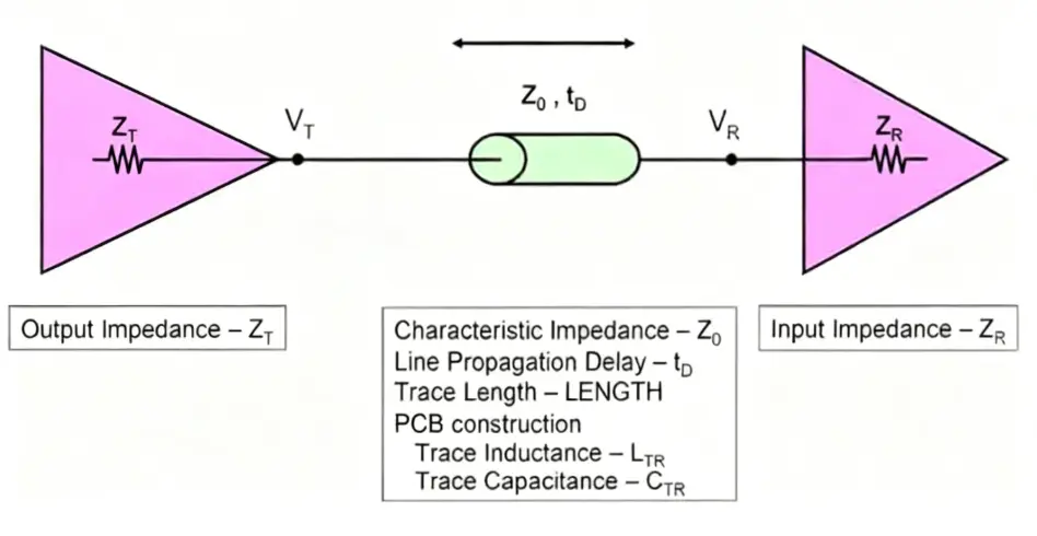
In systems such as computing and telecommunications equipment, signals travel from drivers to receivers via PCB traces. To preserve waveform quality, the trace's characteristic impedance (Z0) must closely align with the input and output impedances of connected components.
3. Key Elements Influencing PCB Impedance Calculation and Trace Characteristics
Several factors influence the impedance of a PCB trace:
-
Dielectric Constant (ER): The dielectric constant of a PCB material shares an inverse relationship with the trace's characteristic impedance.
-
Dielectric Thickness (H): The thickness of the dielectric layer separating the signal trace from the reference plane exhibits a direct relationship with the impedance value.
-
Trace Width (W1, W2): The widths of the impedance line, specifically the bottom (W1) and top (W2) measurements, are inversely related to the characteristic impedance.
-
Copper Thickness (T): There is an inverse relationship between the thickness of the copper trace and the resulting characteristic impedance.
-
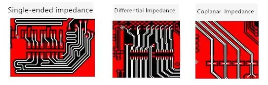
Trace Spacing (S): For differential pairs, the spacing between the two adjacent traces shows a direct relationship with the differential impedance value.
-
Solder Mask Thickness (C): The thickness of the solder mask applied to the PCB substrate is inversely related to the impedance.
4. Manufacturing Process Considerations for PCB Impedance Control
-
When copper thickness exceeds 2oz, PCB impedance becomes difficult to manage due to variations introduced by etching.
-
In designs where certain areas lack copper or wiring layers, prepreg is used to fill gaps during fabrication. For impedance calculations, the dielectric thickness specified by the material supplier cannot be applied directly. Instead, the thickness occupied by the prepreg in these empty sections must be deducted. This discrepancy often explains why in-house impedance calculations differ from those provided by the manufacturer.
5. Guidelines for Using PCB Impedance Calculators
Impedance calculation for PCBs can be complex, but established guidelines help accelerate the process:
-
For standard FR4 substrates, a 50-ohm microstrip typically requires a trace width double the dielectric thickness.
-
Conversely, a 50-ohm stripline generally needs a width about half the total dielectric distance between its reference planes.
These ratios assist in quickly estimating initial trace dimensions, with the precise calculated width often being slightly narrower. While efficiency is important, accuracy remains critical. Discrepancies between designer calculations and manufacturer results are common. Maintaining oversight of these parameters ensures superior product quality and reduces dependency on external corrections.
How Do We Control PCB Impedance in Design?
Three Common Approaches
1. Utilize Historical Impedance Parameters:
Using past PCB designs (trace width, board thickness) as a reference database for future designs. This ensures consistency and efficiency but carries significant risk. If the stack-up parameters of the PCB are changed, the impedance will also change, making this method unreliable.
2. Mark Traces for Factory Control:
Standard practice involves clearly marking impedance-controlled traces in the PCB layout and sharing the annotated design files with the PCB manufacturer, who then fine-tunes parameters like trace width and spacing to meet the targets. While common, this approach can lead to problems. PCB Factory engineers may call to say the impedance can't be achieved because the required adjustments to line width and spacing cannot be accommodated within the available space on the PCB.
3. Pre-Calculation with Manufacturer's Stack-Up Data (The Safest Method):
During the design phase, impedance lines are calculated using specialized software (e.g., si9000) based on the PCB fabricator's provided stack-up data (materials, dielectric constants, solder mask, prepreg thickness). The final design data is then sent for production with clear impedance control requirements. This approach minimizes the need for manufacturer adjustments, as the initial design is already highly accurate. The third scheme is the safest, preventing the PCB Factory from being unable to control the impedance.
Advanced Tools for Impedance Calculation
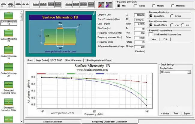
Polar Instruments Si8000 Field Solver
A widely adopted impedance modeling application in the PCB sector is Polar Instruments' Si8000 Field Solver. This advanced tool utilizes a boundary element method for electromagnetic simulation. It offers multiple predefined impedance structures, allowing engineers to derive results by choosing the appropriate template and entering parameters like trace width, spacing, dielectric thickness, copper weight, and dielectric constant.
Opal's Inplan Platform for Automation
-
PCBs often require numerous impedance profiles—ranging from just a few to over twenty unique configurations—each with distinct specifications. Manually validating data and entering each set of parameters individually is labor-intensive and increases the likelihood of inaccuracies.
-
Opal's Inplan platform enables automated PCB impedance design, significantly boosting efficiency prior to manufacturing. The Orbotech Inplan solution integrates with the Si8000 tool to perform impedance calculations driven by a structured database. This begins with creating a comprehensive material library within Inplan, categorized by PCB supplier and material type, and incorporates actual production parameters (laminated thickness, base copper thickness, prepreg resin content) to ensure accurate modeling.
-
The software automatically configures impedance calculation parameters for in-plane structures based on copper weight, impedance models, and layer position. With a single command, results for any number of impedance groups are delivered within seconds.
PCBMO's Impedance Control Process
At PCBMO, our impedance calculation procedure is as follows:
-
Specification Sheet: Manufacturing Instruction (MI) engineers complete a specification sheet based on the computed results, detailing parameters like target impedance, reference layer, trace width, and test point requirements.
-
Coupon Creation: CAM engineers utilize this data to either manually create impedance coupons or employ automated scripts for generation. Typically, each distinct impedance value specified requires a dedicated coupon.
-
Impedance Coupon: As a PCB manufacturer, if the client does not provide a custom impedance coupon, we will design one and position it along the board edge or a breakaway tab (subject to client approval). This coupon is designed to match all specified impedance parameters of the customer's PCB. Testing the impedance coupon provides verification that the impedance control on the actual board meets design requirements.
In the increasingly competitive PCB industry, sample lead times are continuously shrinking. Impedance control is a critical part of pre-production engineering, making the acceleration of impedance tuning and the achievement of precise matching essential priorities. To define impedance specifications, engineers can utilize a dedicated PCB impedance calculator for accurate pre-layout planning.