What is PCB assembly?


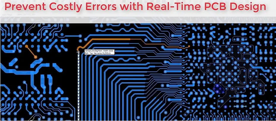
Outline of PCBA Assembly Process Documentation: From Stencil Fabrication to Final Cleaning

This document provides a comprehensive step-by-step guide to the PCBA (Printed Circuit Board Assembly) process, from the initial design review to the final cleaning of the assembled board.

1. Review of Design Files and Quote

This initial phase is foundational to the success of PCBA assembly. The core purpose is to clarify customer requirements and ensure the accurate implementation of the entire PCBA processing workflow.

1.1 Design Files Required from Customers

To achieve this, specific design files must be provided by the customer:
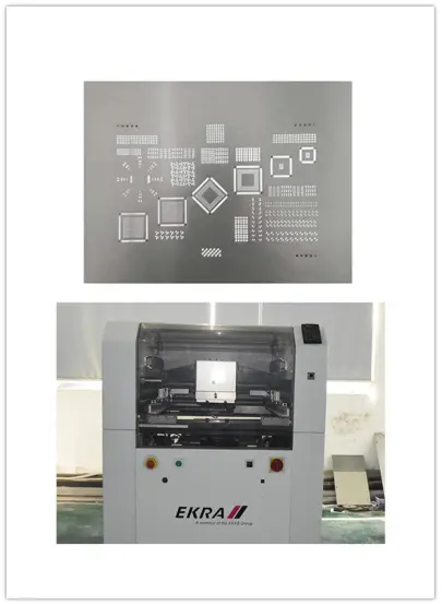
  • Gerber Files: A universal format for PCB design, containing comprehensive details about the board's layout and component placement. These files serve as the primary reference for precise assembly operations.

  • Bill of Materials (BOM): Enumerates all necessary components—including part numbers, quantities, tolerances, and manufacturer information—which directly guides the component procurement process to avoid shortages or mismatches.

  • Assembly Drawings: Offer detailed assembly instructions, specifying component placement requirements and any special technical specifications to eliminate ambiguities during hands-on work.

  • Test Plans: Outline the testing requirements for the finished product, laying the groundwork for subsequent quality verification and ensuring the final PCBA meets predefined performance standards.

                                                                                                                        Gerber file


2. Stencil Fabrication

Stencil fabrication is a key preparatory step for solder paste application, involving the use of a thin sheet of metal or other durable materials with precision-cut openings corresponding to the component pads on the PCB.

2.1 Process Steps

The process follows a systematic sequence:

  1. The stencil is tightly secured over the PCB to ensure alignment.

  2. A squeegee is used to apply solder paste across the stencil surface, forcing the paste through the pre-cut openings.

  3. Excess solder paste is then removed, leaving a uniform layer of solder paste only on the designated pads of the PCB.

2.2 Process Importance

This process is vital because it directly ensures the accuracy of solder paste dosage and even application—two factors that are indispensable for establishing reliable electrical and mechanical connections between components and the PCB, as well as guaranteeing the long-term stable operation of the assembled board.

2.3 Quality-Influencing Factors

Several factors influence stencil quality:

  • Stencil Thickness: Affects the smoothness of solder paste application.

  • Stencil Material: Determines its durability and service life, with different materials offering varying levels of wear resistance.

  • Solder Paste Characteristics: The particle size and composition of the solder paste impact application precision and post-soldering connection reliability.

  • Opening Precision: The precision of the stencil openings directly dictates the overall quality of solder paste deposition.

                                                                                                              Stencil Fabrication


3. Dispensing Solder Paste

Solder paste is a viscous mixture composed of fine solder particles, flux, and a paste-like binder, designed to fulfill two core functions in PCBA assembly.

3.1 Process Functions
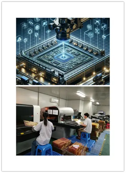
  • Temporary Mechanical Fixation: Holds components securely in place during the subsequent heating process to prevent displacement.

  • Provide Soldering Heat: When heated, the solder within the paste melts, facilitating the formation of permanent electrical and mechanical connections between components and the PCB.

3.2 Subsequent Processes

Following solder paste dispensing, the process proceeds to component placement—where electronic components are aligned precisely with the solder paste-covered pads—before moving to reflow soldering. In the reflow oven, controlled heating melts the solder paste, and upon cooling, it solidifies to form robust, long-lasting connections.


4. Automated Component Placement

This phase is the core of efficient and precise PCBA assembly, leveraging pick-and-place machines to position electronic components accurately and rapidly at their designated locations on the PCB.

4.1 Process Steps

  1. Generate Placement Plan: Using CAD software, engineers develop a detailed scheme specifying the exact position and orientation of each component based on the PCB's structural design.

  2. Component Pickup: The pick-and-place machine (or robotic system) retrieves individual components from trays or tape reels—common packaging formats for electronic components—with high-precision suction nozzles.

  3. Precise Placement: The machine places each component onto the pre-dispensed solder paste pads on the PCB, adjusting the component's orientation through rotation or flipping as required to ensure perfect alignment with the pads.

4.2 PCBmo's Advantages

PCBmo excels in this process by adopting the latest technologies and state-of-the-art equipment, paired with a team of professional technicians. This enables the company to handle complex and high-demand projects that require meticulous component placement and strict quality control.


5. Reflow Soldering

Reflow soldering is a critical bonding process that uses high-temperature heating to melt the solder paste, creating firm and reliable electrical and mechanical connections between surface-mounted electronic components and the PCB. It is specifically designed for surface-mounted boards.

5.1 Process Types

  • Single-sided mounting: For PCBs with components on one side.

  • Double-sided mounting: For PCBs with components on both sides.

5.2 Key Equipment

The key equipment for this phase is a reflow oven—a specialized heating chamber that regulates temperature in precise stages.

5.3 Process Parameters

The critical process parameters include a heating temperature range of 220-260°C (428-500°F) , with strict control over both the heating and cooling cycles. This precise temperature management ensures that the solder paste melts evenly and forms strong, defect-free joints without damaging sensitive components.
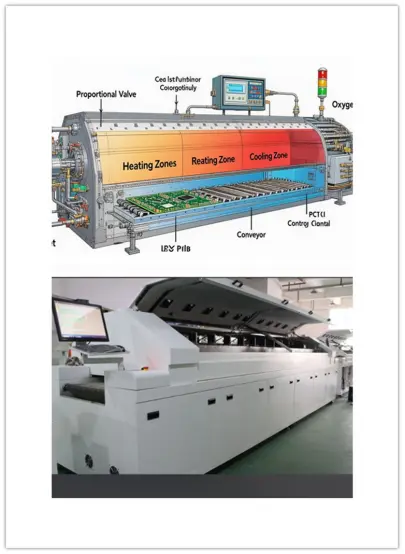


6. Quality Control and Inspection

Quality control and inspection are integral to ensuring that finished PCBA products meet rigorous standards for performance, reliability, and safety, while identifying and correcting any defects early in the production process.

6.1 Inspection Methods

A multi-faceted inspection approach is employed to cover all potential issues:

  • Visual Inspection: Examining the PCB with the naked eye or a magnifying glass to detect visible defects such as component misalignment, soldering flaws, and physical damage.

  • Automated Optical Inspection (AOI): Utilizes specialized high-resolution cameras and advanced software to automatically scan the PCB, identifying subtle defects like tiny solder bridges or component polarity errors.

  • In-Circuit Testing (ICT): Employs specialized equipment to test the electrical characteristics of the PCB and its components within the circuit, verifying continuity, resistance, and capacitance.

  • Ultrasonic Testing: Uses high-frequency sound waves to detect internal defects that are inaccessible to visual or optical methods, such as delamination or hidden solder voids.

  • X-ray Inspection: Leverages X-ray imaging technology to inspect the internal structure of the PCBA, ideal for detecting:

    • Soldering defects (shorts, opens, bridging)

    • Misaligned or improperly positioned components

    • Missing or damaged components

    • Internal damage or defects within components


7. Placement and Soldering of Through-hole Components

Also known as Plated Through Holes (PTH) or DIP (Dual In-line Package) assembly, this process is designed for components with leads that pass through holes drilled in the PCB.

7.1 Process Steps

  1. Manual Insertion: Component leads are carefully threaded through the corresponding PCB holes and aligned in the correct position.

  2. Fixation and Positioning: Jigs are used to secure the components in place, preventing movement during soldering.

  3. Soldering Connection: Leads are soldered to the PCB using either a soldering iron for small-scale production or wave soldering for high-volume manufacturing.

7.2 Process Control

Strict process control is essential, with precise regulation of temperature and soldering time to avoid overheating or insufficient soldering.

7.3 PCBmo's Principle

PCBmo tailors the wave soldering temperature to the specific characteristics of each component, ensuring accurate and reliable component positioning and soldering, thereby guaranteeing the overall functional reliability of the PCBA.
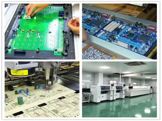


8. Functional Testing

Functional testing is conducted at the final stage of PCBA production to verify that the assembled board operates as intended. The testing scope covers both individual components and the entire assembly.

8.1 Testing Technologies

Three core testing technologies are employed:

  • Input/Output Testing: Verifies whether the PCBA's ability to receive input signals and generate corresponding output responses complies with the original design specifications.

  • Performance Testing: Evaluates the PCBA's performance under various operating conditions to ensure it meets key performance indicators such as speed, efficiency, and stability.

  • Stress Testing: Subjects the PCBA to extreme environmental conditions (e.g., high/low temperatures, humidity, vibration) to simulate real-world usage and verify its durability and reliability over time.

8.2 Requirements for Test Fixtures

Test fixtures play a crucial role, requiring the ability to accurately and reliably fix the PCBA, facilitate easy access to test points, and withstand the rigors of the test environment.

8.3 Supported Fixture Types

  • Test Jigs: Manually or automatically operated fixtures that secure the PCBA and provide access to components and connections for testing.

  • Socket Fixtures: Equipped with dedicated sockets designed to hold specific component types (e.g., integrated circuits), allowing for easy component replacement during testing without rework.

  • Probes: Specialized tools that establish electrical connections with specific test points on the PCBA, enabling targeted testing of individual components or connections.

8.4 PCBmo's Services

PCBmo assists customers in preparing customized test fixtures and conducts local testing before PCBA shipment to ensure that all finished products meet the highest quality standards.
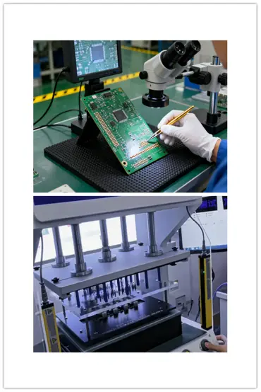


9. PCBA Board Final Cleaning

Final cleaning is the concluding step in PCBA production, with the primary goal of removing residual contaminants and residues (such as excess solder flux, dust, or oil) from the PCBA surface. This improves appearance and prevents interference with electrical performance or long-term reliability.
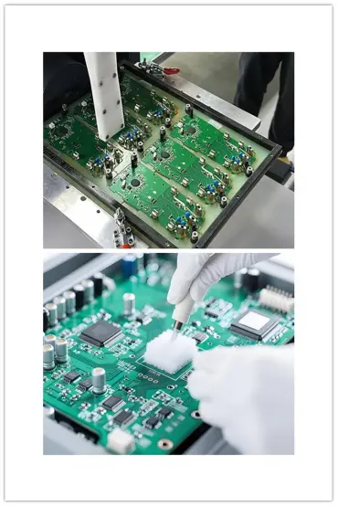

9.1 Cleaning Methods

Three main cleaning methods are available, with selection based on the PCBA's specific requirements and the materials used in production:

  • Solvent Cleaning: Utilizes solvents such as isopropyl alcohol to dissolve and remove contaminants, offering strong cleaning power for stubborn residues.

  • Aqueous Cleaning: Employs water-based cleaning solutions, which are typically milder and less likely to damage sensitive components, making them suitable for PCBs with specific material constraints.

  • Mechanical Cleaning: Uses physical means such as brushes or air jets to dislodge and remove contaminants, ideal for removing dry debris or surface dust without chemical exposure.


Get a Competitive Quote for Your Project

Welcome! Send the Gerber file to me and let me help you review it first. Then, I will try my best to send a more competitive quotation to you.

Quick Turnaround Times:

  • 2-layer PCB: 24 hours

  • 4-layer PCB: 48 hours

  • 6-layer PCB: 72 hours

If you have any questions, please feel free to contact me at any time.