Professional PCB Layout: Definition, Design Process, and PCBmo's Comprehensive Solutions
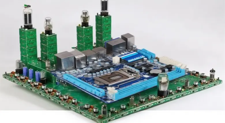
PCB Layout is the process of translating a circuit schematic diagram into a physical printed circuit board design that fulfills the functional requirements specified by circuit designers. An outstanding PCB Layout design not only optimizes production costs significantly but also enhances the overall performance and reliability of the PCBA (Printed Circuit Board Assembly) .
As a crucial component of hardware design, PCB Layout plays a decisive role in determining the final product performance, assuming the hardware circuit design itself is rational. Currently, most PCB layout engineers execute their work in accordance with constraint rules formulated by senior engineers or product hardware engineers, ensuring consistency and compliance with industry standards.
Why Choose PCBmo for Your PCB Layout?
PCBmo stands out as a leading provider of exceptional PCB layout services, backed by years of industry expertise and a commitment to excellence.
-
Comprehensive Capabilities: From minimizing layer counts for high-volume, cost-sensitive products to tackling the complexity of 48+ layer circuit boards.
-
Specialized Expertise: Extensive experience in designing noise-sensitive sections of PCB layouts, a critical factor in ensuring signal integrity and overall product stability.
-
Certified Quality: We hold ISO 9001 quality management system certification (Certification No.: 68626Q00015R000) and comply with IPC-A-600 standards, underscoring our dedication to adhering to global industry benchmarks.
Our Specialist Design Solutions
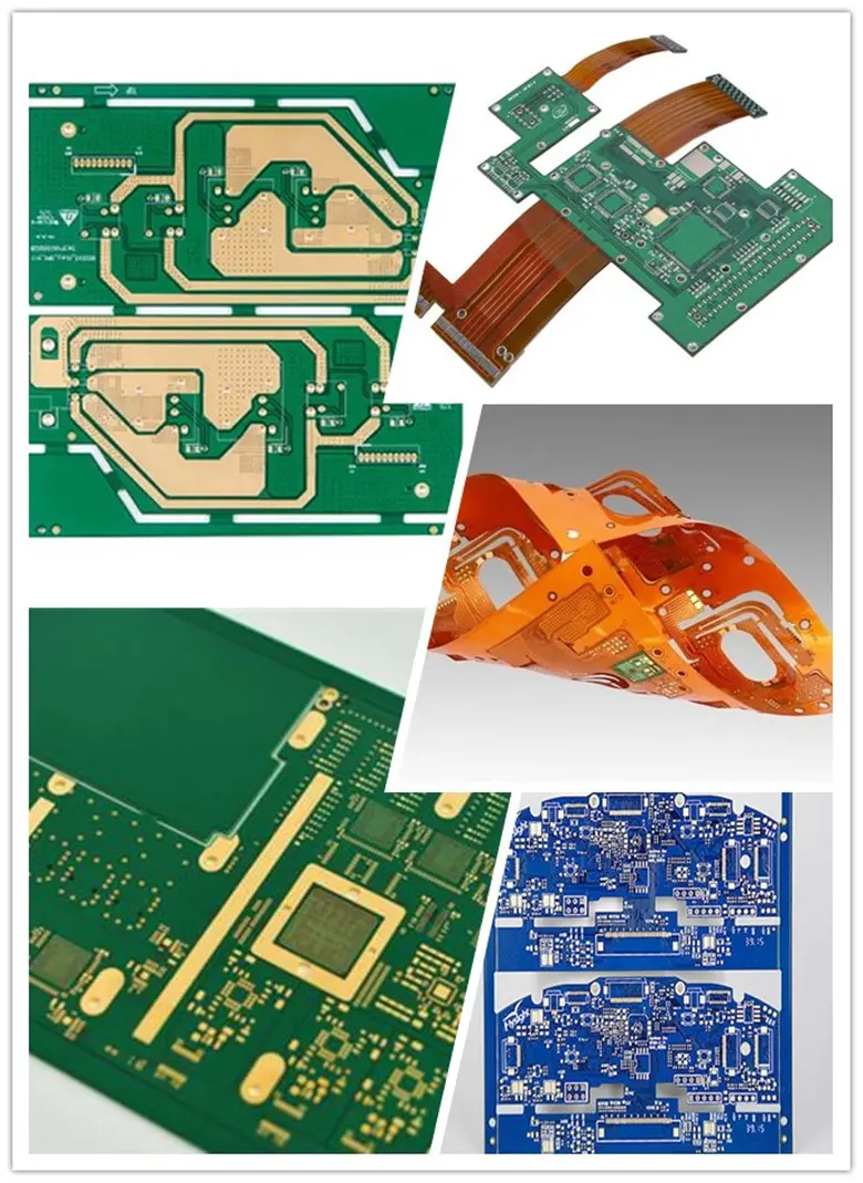
Our specialist design solutions cover all aspects of PCB layout, encompassing a diverse range of board technologies:
-
Single-layer PCB, 2-layer PCB, and Multilayer PCB
-
High-speed Backplanes PCB
-
Rigid-Flex PCB and Flexible PCB
-
HDI (High-Density Interconnect) PCB
-
Blind & Buried Micro-Vias PCB
-
Stacked Micro-Via Impedance Controlled PCB
-
Matched Lengths/Timings Optimization
-
Analogue and Digital Signal Coexistence Design
-
Crosstalk and Timing Controlled Layout
-
Signal Integrity Analysis and PCB Simulation
-
Differential / Balanced Pairs Routing
A Step-by-Step Guide to PCB Layout Design
Creating an effective PCB layout from a circuit diagram requires a systematic approach, adhering to core principles and best practices to ensure functionality, performance, and manufacturability.
1. Core Requirements and Fundamental Principles
The primary requirement of PCB layout is to guarantee the effective connection of all networks. Beyond connectivity, the layout must address distinct signal needs:
A key principle for reasonable component placement is clear modular division. Individuals with basic circuit knowledge should be able to identify the functional purpose of each section at a glance, simplifying debugging, maintenance, and design scalability.
2. Specific Design Workflow
-
Initial File Generation & Pre-Layout: Generate the initial PCB file from the schematic. Complete the pre-layout phase to determine a preliminary PCB area, then collaborate with the mechanical structure team to align the layout with structural constraints.
-
Wiring Layer Planning: Before initiating wiring, gain a comprehensive understanding of the PCB’s cascade design.
-
Classify layers into optimal, suboptimal, and auxiliary.
-
Designate adjacent layers as complete ground planes to minimize interference.
-
Reserve optimal layers for critical signals (e.g., DDR, differential, analog).
-
Route non-critical signals (e.g., I2C, UART, SPI) on other layers.
-
Board Definition & Connector Placement: Draw board edges, positioning ports, and forbidden zones in line with structural constraints. Place connectors strategically to ensure accessibility and compatibility.
3. Component Placement Principles
-
Master MCU Placement: Position the master MCU (Microcontroller Unit) at the center of the board to minimize signal path lengths.
-
Interface Circuit Placement: Place interface circuits (e.g., Ethernet, USB) close to their respective connectors, following the "protection before filtering" principle for ESD protection.
-
Power Module Placement: Place main power modules at the power entrance. Discrete power modules can be placed in areas with dense distribution of the same power network to optimize delivery and reduce voltage drop.
4. Power Circuit Design Considerations
Power circuits must first ensure adequate current-carrying capacity. From an EMC (Electromagnetic Compatibility) perspective, the entire return path should be as thick and short as possible. A long or narrow return path forms a loop antenna. Minimizing the loop area is critical to reducing EMC risks.
5. Internal Circuit Zoning Strategies
Adhere to basic zoning principles for internal circuits:
-
Separate high-speed and low-speed circuits.
-
Isolate analog and digital circuits.
-
Segregate interference sources from sensitive receptors.
This zoning minimizes cross-interference, ensuring each circuit section operates within its optimal environment.
6. Circuit Module Layout
For individual circuit modules, follow the current flow direction during design to optimize signal integrity and reduce signal delay, ensuring consistent performance and simplifying troubleshooting.
PCBmo’s Advanced Methodology & Technical Capabilities
PCBmo’s proven methodology is engineered to meet stringent product requirements, including performance, time-to-market, unit cost, and manufacturing yield.
Pre & Post PCB System Level Signal Integrity Services
We leverage advanced simulation tools to provide a "right first-time" guarantee in critical areas such as impedance control, crosstalk reduction, and signal integrity. Our comprehensive signal integrity solutions include:
-
Timing and Crosstalk Analysis
-
Topology and Termination Strategy Development
-
Design Guideline Generation
-
Margin Analysis (SI and Timing)
-
Stack up and Routing Guideline Formulation
-
Decoupling and Power Delivery Analysis
-
Ball/Bump/Pad Assignment Optimization
-
Design Reviews adhering to good engineering practices
-
2D/3D Electromagnetic Modeling and Simulation
-
Clock System Design and Review
-
I/O Buffer Selection and Validation
Our simulation results are validated against industry standards (e.g., IPC-2221) and backed by third-party testing reports (available upon request via our official website).
Typical Service Deliverables
PCBmo’s engineering team collaborates closely with clients to deliver end-to-end solutions, including:
-
Collaborating with customers to understand system environments.
-
Developing critical signal quality check protocols.
-
Pre-layout solution space analysis and decoupling strategy definition.
-
Pre/post-layout power system design and analysis.
-
Library development (IO buffers, Interconnect, Package, Connectors).
-
Post-layout verification of physical and electrical design rules.
-
Power Integrity Analysis.
Expert Team & Software Proficiency
PCBmo boasts a professional PCB design team with an average of over 10 years of industry experience, including senior engineers with more than 15 years of specialized expertise. Our engineers are proficient in industry-leading software tools such as:
-
Cadence Allegro 17.4
-
Pads 9.5
-
PROTEL DXP
This enables us to independently complete PCB layout designs for a wide range of electronic products, including PC motherboards, industrial control boards, medical devices, mobile phones, and high-speed digital-analog hybrid circuits.
Supported Buses & High-Speed Serial Lines
We have extensive experience working with a diverse range of buses and high-speed serial lines, ensuring compatibility across various applications:
-
Standard Buses: I2C, SPI, CAN, ISA, EISA, VME, VPX, RS232/485/422, USB.
-
High-Speed Serial Buses: PCIe, SATA, SAS, SFP, XAUI, etc., with operating frequencies ranging from 1.5Gbps to 28Gbps and signal rates up to 1G-10G.
Industry-Specific PCB Layout Solutions
PCBmo’s expertise spans multiple industries with tailored solutions designed to address unique challenges.
-
Industrial Control Projects: Rich experience in PLC, DCS, CNC, and high-power x86/ARM architectures (Haswell, Sandy Bridge, Core, Bay Trail processors), ensuring reliability in harsh environments.
-
Communication Equipment: Over 10 years of experience in high-speed PCB design for main control platforms (FBGA, ARM, DSP) with expertise in CPCI, ATCA, VME, and PXI. Extensive experience processing SFP10G optical ports and high-speed signals (3.125G up to 10G) with a focus on crosstalk reduction and loss control.
-
Consumer Electronics: Specialization in HDI blind hole design for main control platforms including Intel, Qualcomm, and Rockchip (RK) processors. Proven expertise in RF signal processing (2.4G/5G WiFi, GPS, 3G, IQ signals) and electrostatic protection compliance (IEC61000-4-2, GB17626.2).
-
Security Camera Products: Prioritizing signal integrity and EMI control for Hisilicon and TI processors. Expertise in high-definition network cameras and NVR matrices, ensuring video and audio signals are routed away from heat and interference sources.
-
Automotive Electronics: Focus on PCB design for peripheral equipment like onboard computers, dashcams, and dual-lens solutions. Designs adhere to automotive-grade reliability and temperature resistance requirements.
Reverse Engineering Services
PCBmo specializes in PCB reverse engineering for cases where film work or schematics have been lost. Leveraging advanced computerized netlist generators and high-precision scanning, we can handle complex multi-layer PCBs. Our capabilities include creating detailed schematics, developing new layouts, and upgrading obsolete designs. All projects comply with intellectual property laws, with clients required to provide proof of legitimate ownership.
Comprehensive Design Services & Customer Commitment
PCBmo offers a full suite of design services, including PCB layout, simulation, EMC, and principle design.
-
Efficiency: Our rigorous design process helps clients improve R&D efficiency and reduce costs, shortening time-to-market by an average of 30% compared to industry benchmarks.
-
Partnership: In addition to standalone services, PCBmo provides end-to-end physical board solutions. Our team can collaborate with your in-house engineers or offer full turnkey integrated services.
-
One-Stop Service: We also provide seamless services from PCB manufacturing to PCBA assembly, streamlining the supply chain and improving product reliability.
Contact Us
For more information about our services, case studies, or to request a consultation, visit our official website or contact our technical support team.
References
-
IPC-2221, "Generic Standard on Printed Board Design", IPC Association Connecting Electronics Industries, 2022.
-
Cadence Design Systems, "Allegro PCB Designer User Guide", Version 17.4, 2023.
-
PCBmo Official Technical Whitepaper, "PCB Layout Best Practices for High-Speed Circuits", 2024, Version 2.1.
-
GB17626.2, "Electromagnetic Compatibility (EMC) - Part 4-2: Testing and Measurement Techniques - Electrostatic Discharge Immunity Test", Standardization Administration of China, 2021.