PCB Procurement Guide: Materials, Classification, Process & Trends
1. Introduction to PCB
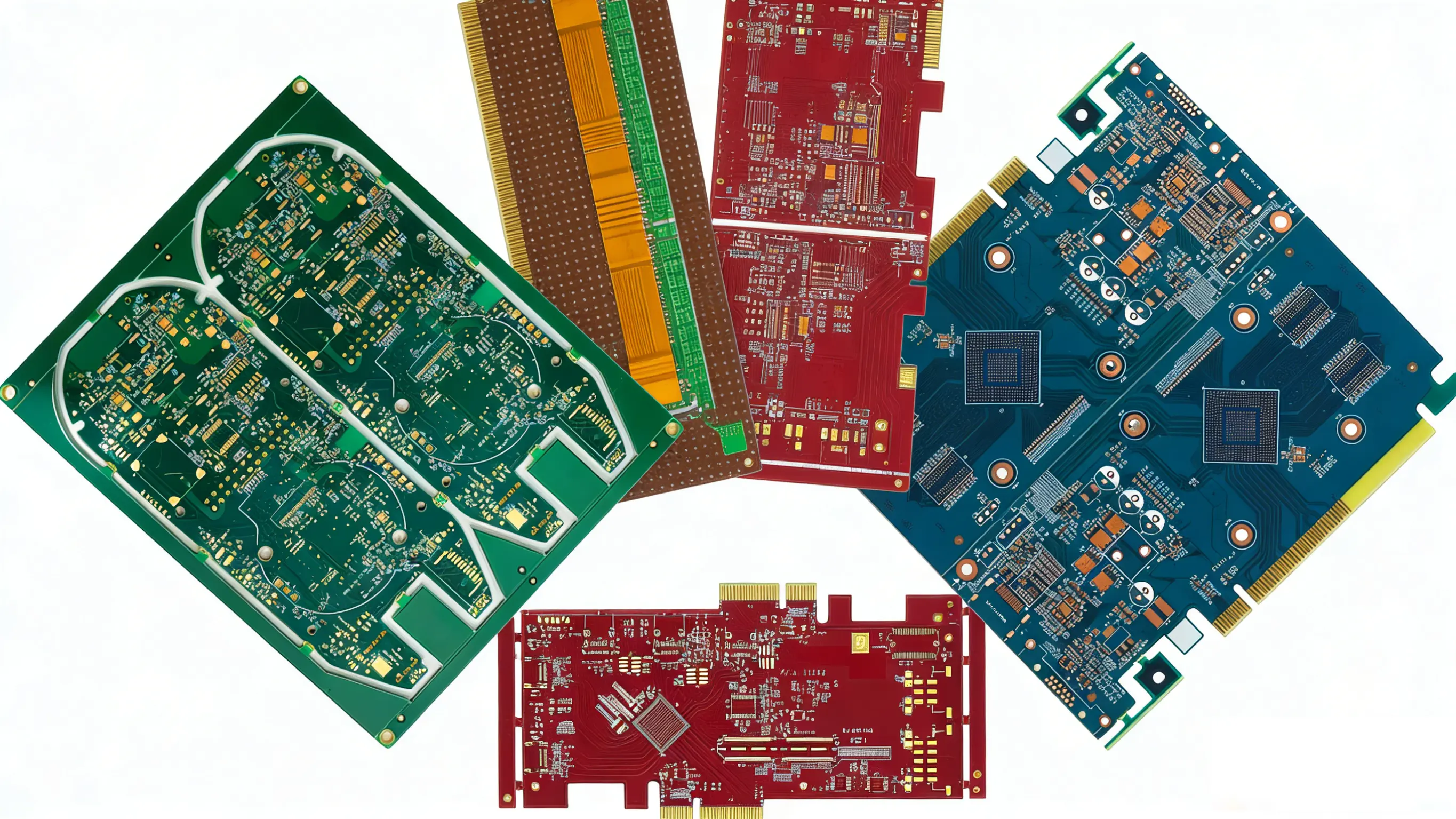
A Printed Circuit Board (PCB) is a fundamental electronic component that provides both mechanical support and electrical connections for electronic components. This is achieved through conductive pathways etched from copper sheets laminated onto a non-conductive substrate. Serving as the "backbone" of electronic products, PCBs are utilized across a vast array of industries. A solid understanding of PCB knowledge is essential for efficient and high-quality procurement. This guide systematically organizes core PCB information from multiple perspectives to assist beginners in navigating the procurement process effectively.
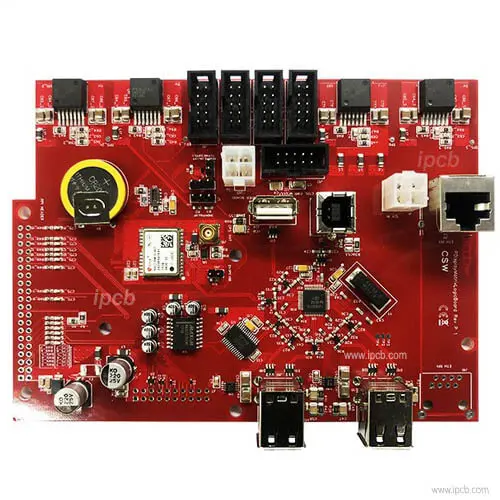
PCB - Printed Circuit Board
2. PCB Materials
The performance characteristics and application scope of a PCB are directly determined by its constituent materials. The primary materials include the substrate, copper foil, solder mask ink, and silkscreen ink, with the substrate being the most critical element.
2.1 Substrate Materials
The substrate is the foundational layer of a PCB, responsible for supporting components and providing electrical insulation. Common types include:
-
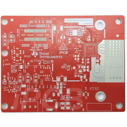
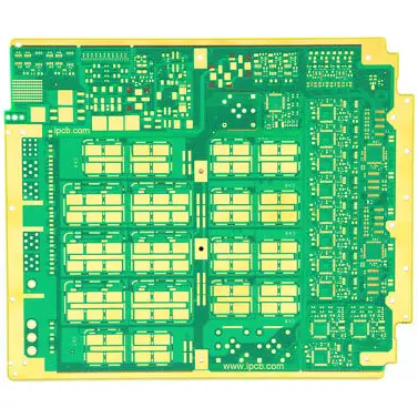
FR-4: This is the most widely used epoxy resin glass fiber substrate. It offers excellent mechanical properties, electrical insulation, and heat resistance, making it suitable for most general electronic products like consumer electronics, industrial control equipment, and communication devices. Its cost-effectiveness makes it the preferred choice for mass production.
-
FR-1/FR-2: These are phenolic resin paper substrates. While they have a low cost, their heat resistance is poor. They are primarily used in low-end electronic products with simple functions and low operating temperatures, such as toys and basic household appliances.
-
Aluminum-Based PCB: These substrates use aluminum as a base with an insulating layer in between. They provide superior heat dissipation, making them ideal for high-power electronic products that generate significant heat, such as LED lighting, power supplies, and automotive electronics.
-
Ceramic PCB: Made from ceramic materials like alumina or aluminum nitride, these substrates offer exceptionally high heat resistance, insulation, and thermal conductivity. Due to their high cost, they are mainly used in specialized fields like aerospace, military electronics, and high-frequency communication, where precision and temperature resistance are paramount.
2.2 Copper Foil
Copper foil is the conductive material used to create the circuit patterns on a PCB. Based on the manufacturing process, it is categorized as:
-
Electrolytic Copper Foil: This type has a low cost, high production efficiency, and high purity. It is widely used in general PCBs. Its relatively high surface roughness improves the bonding force with the substrate.
-
Rolled Copper Foil: It offers better flexibility, ductility, and conductivity. This makes it suitable for Flexible PCBs (FPC) or products requiring frequent bending, such as mobile phone folding screens and wearable devices. Its cost is higher than that of electrolytic copper foil.
2.3 Solder Mask Ink
Solder mask ink is applied to the PCB surface to protect the circuits, prevent short circuits caused by solder bridging during assembly, and resist moisture, dust, and corrosion. Common colors include green, red, blue, and black. Green is the most prevalent due to its good contrast, which facilitates circuit inspection.
2.4 Silkscreen Ink
Silkscreen ink is used to print component labels, pin numbers, and manufacturer information on the PCB surface. This aids in component assembly, maintenance, and identification. It is typically white or black for good visibility.
3. PCB Classification
PCBs can be classified into different types according to various standards, which is crucial for defining procurement requirements accurately.
3.1 Classification by Substrate Rigidity
-
Rigid PCB (RPCB): The substrate has high rigidity and cannot be bent. Most electronic products, such as computer motherboards, TV mainboards, and automotive electronic control modules, use rigid PCBs. FR-4 and aluminum-based substrates are common materials.
-
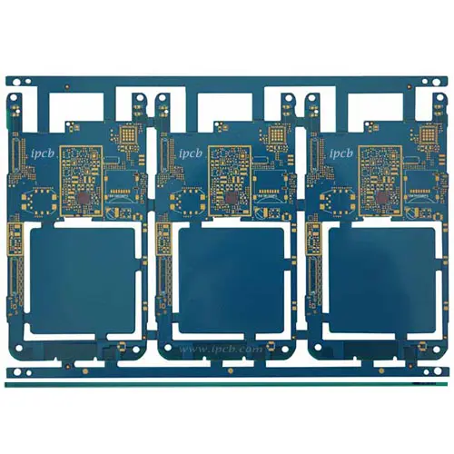
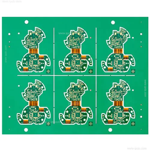
Flexible PCB (FPC): The substrate is made of flexible materials like polyimide (PI) or polyester (PET), allowing the board to be bent, folded, or twisted. It is ideal for products with limited space or requiring movement, such as mobile phone cameras, wearable devices, and automotive wiring harnesses. FPCs are lightweight, thin, and offer high integration.
-
Rigid-Flex PCB (RFPCB): This is a combination of rigid and flexible PCBs, integrating the advantages of both. Rigid sections provide support for components, while flexible sections act as interconnections and adapt to spatial layouts. They are widely used in high-end electronics like aerospace equipment, medical devices, and advanced mobile phones.
3.2 Classification by Number of Layers
-
Single-Sided PCB: The circuit is present on only one side of the substrate. It has a simple structure, low cost, and low production difficulty. It is suitable for simple electronic products with few components, such as radio circuits, simple power supplies, and toy controls.
-
Double-Sided PCB: Circuits are on both sides of the substrate, connected by plated-through holes (vias). It allows for a higher component density than single-sided boards and is widely used in consumer electronics like mobile phones, tablets, and household appliances.
-
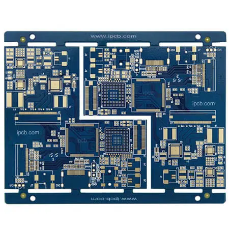
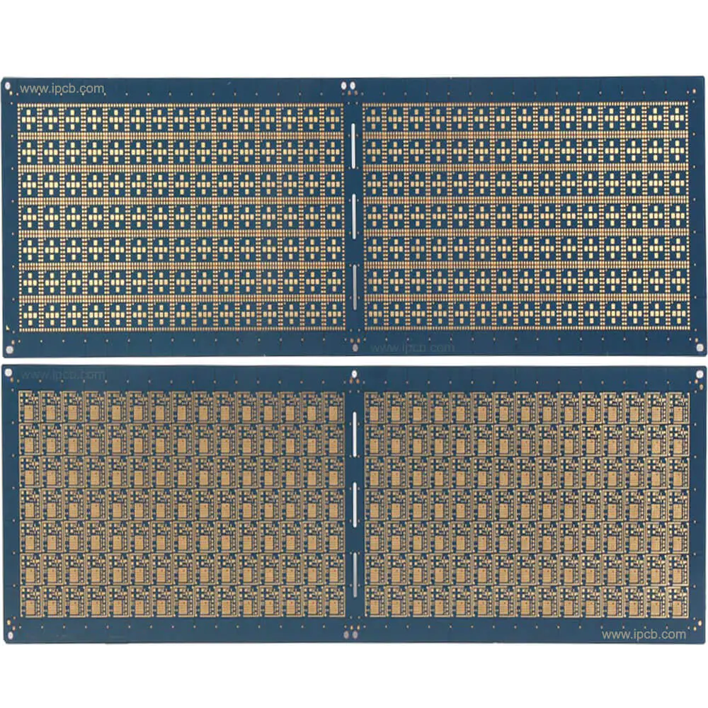
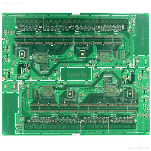
Multilayer PCB: Consisting of three or more conductive layers, each separated by insulating material, the layers are interconnected using various via types (through-hole, blind, buried). They offer high integration, compact size, and good electromagnetic compatibility. They are essential for high-precision, complex products like computer motherboards, server boards, communication base stations, and aerospace electronics. Common configurations include 4-layer, 6-layer, 8-layer, and 12-layer boards.
3.3 Classification by Conductive Pattern and Structure
-
Standard PCB: The traditional PCB with etched copper foil forming the conductive pattern, suitable for most general electronic products.
-
High-Frequency PCB: Designed for high-frequency signal transmission (typically above 1GHz), these boards feature low dielectric loss and stable electrical performance at high frequencies. Common materials include PTFE (Teflon) substrates. They are used in communication equipment such as 5G base stations, radar, and satellite communication systems.
-
Heavy Copper PCB: With a copper foil thickness greater than 35μm (often 70μm-140μm), these boards have a high current-carrying capacity and superior heat dissipation. They are suitable for power electronics like power supplies, inverters, and electric vehicle controllers.
4. PCB Design
PCB design is a critical phase that influences the performance, reliability, and manufacturability of the final product. Understanding basic design requirements is helpful for formulating realistic and effective procurement specifications.
4.1 Design Principles
-
Electromagnetic Compatibility (EMC): This involves the rational arrangement of components and circuits to minimize electromagnetic interference (EMI) and improve electromagnetic susceptibility (EMS). Examples include separating analog and digital circuits and incorporating ground planes.
-
Thermal Design: For components generating significant heat (e.g., power chips), they should be placed in areas with good heat dissipation. Designing thermal pads or thermal vias ensures the PCB operates within a safe temperature range.
-
Design for Manufacturability (DFM): The design must adhere to PCB production process capabilities, such as using reasonable line widths and spacings, appropriate via sizes, and sufficient solder mask clearance. This reduces production difficulties and defect rates.
-
Reliability: Ensuring the PCB's mechanical strength, avoiding stress concentration points, and selecting appropriate materials and processes based on the intended operating environment (e.g., high temperature, humidity, vibration) are key for long-term reliability.
4.2 Common Design Software
Common PCB design software includes Altium Designer, KiCad, Eagle, OrCAD, and PADS. Different software has its own features. When procuring, it's necessary to confirm that the supplier can accept design files in the required format, with Gerber files being the standard format for PCB production.
5. PCB Manufacturing Process
Understanding the PCB manufacturing process aids in evaluating a supplier's production capacity and quality control level, as well as setting reasonable delivery time expectations.
5.1 Main Process of Rigid PCB
-
Substrate Cutting: Large sheets of substrate material are cut into the required panel sizes based on the design.
-
Drilling: Holes (through-holes, blind vias, buried vias) are drilled to enable electrical connections between layers.
-
Copper Plating: A thin layer of copper is chemically plated onto the hole walls and panel surface to create a conductive path.
-
Circuit Pattern Transfer: The desired circuit pattern is transferred onto the PCB using photolithography (applying photoresist, exposure through a mask, and development).
-
Etching: Unwanted copper not protected by the photoresist is chemically etched away, leaving the required circuit pattern.
-
Solder Mask Coating: Solder mask ink is applied over the entire board surface, then exposed and developed to leave solder mask only on areas not meant for soldering.
-
Silkscreen Printing: Component labels, logos, and other markings are printed onto the board using silkscreen ink.
-
Surface Treatment: The exposed copper areas (pads) are treated to improve solderability and protect against oxidation. Common finishes include HASL (Hot Air Solder Leveling), ENIG (Electroless Nickel Immersion Gold), OSP (Organic Solderability Preservatives), and Immersion Silver.
-
Testing: Electrical testing (e.g., for open and short circuits) and visual inspection are conducted to ensure the PCB meets quality requirements.
-
Final Cutting and Packaging: Individual PCBs are cut from the production panel (e.g., using V-grooving or routing), inspected, and then packaged for shipment.
5.2 Key Quality Control Nodes
Critical quality control points during manufacturing include drilling accuracy, uniformity of copper plating thickness, precision of the circuit pattern, solder mask adhesion, quality of the surface finish, and the results of electrical performance testing. Reputable suppliers establish strict quality standards for these nodes and perform in-process inspections.
6. PCB Functions and Applications
6.1 Core Functions
-
Mechanical Support: Provides a stable platform for mounting and securing electronic components.
-
Electrical Connection: Establishes the required electrical interconnections between components via conductive traces, enabling signal and power transmission.
-
Heat Dissipation: Aids in dissipating heat generated by operating components, helping to ensure reliable product performance.
-
Protection: The solder mask and substrate materials shield the circuitry from environmental factors like moisture, dust, and corrosion.
6.2 Main Application Fields
-
Consumer Electronics: Smartphones, tablets, computers, TVs, cameras, wearable devices (smartwatches, fitness trackers). These products often utilize high-density double-sided or multilayer rigid PCBs and flexible PCBs.
-
Automotive Electronics: Engine control units (ECUs), infotainment systems, navigation, LED headlights, battery management systems (BMS) in electric vehicles. Automotive PCBs demand high reliability, heat resistance, and vibration resistance, with aluminum-based and rigid-flex boards being common.
-
Communication Equipment: 5G base stations, routers, switches, optical modules, satellite communication gear. High-frequency PCBs and multilayer boards with excellent electromagnetic compatibility are primary choices here.
-
Industrial Control: Programmable Logic Controllers (PLCs), variable frequency drives, industrial sensors, automation equipment. These PCBs must perform reliably in harsh industrial environments with temperature extremes, humidity, and electrical interference.
-
Aerospace and Military: Aircraft avionics, satellite subsystems, military communication devices. These sectors have the most stringent requirements for materials, reliability, and interference immunity, often using ceramic or high-reliability multilayer PCBs.
-
Medical Devices: Patient monitors, ultrasound equipment, Magnetic Resonance Imaging (MRI) machines. Medical PCBs require high precision, reliability, and in some cases, biocompatibility.
7. PCB Procurement Process
A standardized procurement process helps ensure that the purchased PCBs meet the required quality, cost, and delivery time objectives.
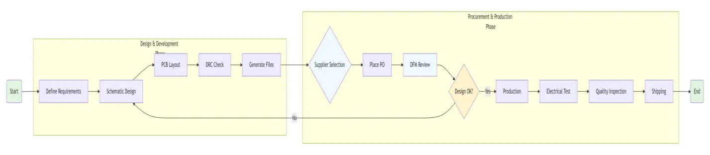
7.1 Demand Definition
First, clearly define the specific PCB requirements, including:
-
Basic Parameters: Type (rigid/flexible/rigid-flex), number of layers, dimensions, and thickness.
-
Material Requirements: Substrate material (FR-4/Aluminum/Ceramic), copper foil thickness, solder mask color, and surface finish type.
-
Design Files: Provide complete design files (e.g., Gerber files, netlist) and technical specifications.
-
Quality Requirements: Tolerances, electrical performance targets, and any required reliability tests (e.g., thermal shock, humidity, vibration).
-
Quantity and Delivery Time: Determine the order quantity (prototype vs. production run) and the required delivery schedule.
7.2 Supplier Selection
Choosing a reliable supplier is critical for procurement success. Key selection criteria include:
-
Qualification and Certification: Check for certifications like ISO9001 (Quality Management), ISO14001 (Environmental Management), IATF 16949 (Automotive), and relevant experience in the target application field.
-
Production Capacity: Evaluate if the supplier's production scale, equipment, and process capabilities (e.g., multilayer board capability, high-frequency experience) align with the requirements.
-
Quality Control: Understand the supplier's quality management system, testing equipment, and typical defect rates. On-site audits for critical suppliers are recommended.
-
Price and Cost Performance: Obtain quotes from multiple suppliers, comparing both price and quality to select a cost-effective partner, avoiding the pitfall of choosing the lowest price at the expense of quality.
-
Delivery Capability: Assess the supplier's ability to meet delivery deadlines, especially for urgent orders. Understand their typical production lead times and contingency plans.
-
After-Sales Service: Understand the supplier's policies for handling quality issues, returns, and providing technical support.
7.3 Quotation and Negotiation
Send the detailed requirements document to selected potential suppliers and request formal quotations. Quotations typically include unit price, total price, payment terms, and delivery time. Conduct in-depth negotiations on these points and quality assurance clauses to reach a mutual agreement.
7.4 Contract Signing
After negotiations, sign a formal procurement contract. The contract should clearly specify:
-
Product Specifications: Detailed PCB parameters, design file references, and technical requirements.
-
Quantity and Delivery: The exact order quantity, delivery date(s), and location.
-
Price and Payment Terms: Total amount, payment method (e.g., deposit, final payment), and payment schedule.
-
Quality Standards and Inspection: The applicable quality standards (e.g., IPC-A-600), acceptance criteria, and inspection methods (buyer's incoming inspection, third-party).
-
Liability for Breach of Contract: Consequences for non-compliance, such as late delivery or quality failures.
-
After-Sales Service Clauses: Procedures for handling quality problems, returns, and exchanges.
7.5 Incoming Inspection
Upon receipt of the PCBs, perform incoming inspection according to the contract and quality standards. Typical inspection items include:
-
Visual Inspection: Check for appearance defects (scratches, solder mask bubbles, silkscreen legibility), dimensions, and thickness.
-
Electrical Performance Test: Use equipment like a flying probe tester to verify no opens or shorts and that critical impedances are met.
-
Reliability Test: For critical products, perform specified tests like thermal aging, humidity resistance, or vibration.
-
If non-conforming products are found, contact the supplier promptly to arrange for return, exchange, or rework as per the contract.
7.6 Payment and Follow-Up
Process the payment according to the contract terms after successful incoming inspection. Maintain communication with the supplier throughout the cooperation, track progress on subsequent orders, and periodically evaluate the supplier's performance (quality, delivery, service) to foster a long-term, stable relationship.
8. PCB Cost Factors
The cost of a PCB is influenced by multiple factors. Understanding these helps in controlling procurement expenses.
8.1 Material Cost
Material cost constitutes a significant portion of the total PCB cost. Prices vary widely: ceramic substrates are the most expensive, followed by aluminum-based and high-frequency substrates (e.g., PTFE), while FR-4 is the most economical. Copper foil thickness, surface finish type (ENIG is more costly than HASL or OSP), and even solder mask color can also affect material cost.
8.2 Design Complexity
Higher design complexity drives up cost. This includes multilayer boards (especially 8+ layers), fine line/space features (e.g., line width ≤ 0.1mm), and a high density of vias, particularly blind and buried vias, all of which require more precise and complex manufacturing.
8.3 Order Quantity
Order quantity has an inverse relationship with unit price. Larger production runs spread fixed costs (like tooling and setup) over more units, lowering the per-unit price. Prototype orders (e.g., 1-10 pieces) typically have a significantly higher unit price than mass production orders.
8.4 Production Process and Surface Treatment
Specialized processes, such as those for high-frequency or rigid-flex boards, require unique equipment and expertise, adding to the production cost. Different surface finishes also have different costs: ENIG is typically the most expensive, followed by Immersion Silver and OSP, with HASL generally being the lowest cost.
8.5 Quality Requirements and Testing Costs
Stricter quality requirements (tighter tolerances, higher reliability standards) necessitate more precise equipment and more comprehensive testing, increasing both production and testing costs. PCBs for aerospace or military use, requiring extensive reliability testing, will have higher associated costs.
8.6 Delivery Time
Urgent orders (e.g., requiring 24-48 hour turnaround) require suppliers to expedite production, often involving overtime and schedule disruptions. This results in additional expediting fees and a higher unit price.
9. Future Trends of PCB
As electronic technology evolves, PCBs are subject to several development trends that will influence future procurement strategies.
9.1 High Integration and Miniaturization
Driven by products like wearables and miniaturized medical devices, PCBs are trending towards higher density and smaller size. This means finer line widths/spaces (potentially below 0.05mm) and an increasing number of layers in multilayer boards, requiring suppliers to possess advanced precision manufacturing capabilities.
9.2 High-Frequency and High-Speed
The advancement of 5G, radar, and satellite communications demands PCBs capable of excellent high-frequency and high-speed signal transmission. The use of high-frequency materials (like PTFE, Liquid Crystal Polymer - LCP) and specialized processes will become more widespread, leading to continued growth in demand for these boards.
9.3 Green and Environmental Protection
Increasing environmental awareness is leading to stricter regulations on electronic products. PCB manufacturers are progressively adopting environmentally friendly materials (e.g., lead-free solder mask, halogen-free laminates) and processes (e.g., water-based etching, energy-efficient equipment). Environmental compliance will become an increasingly important factor in PCB procurement decisions.
9.4 Integration of Multiple Functions
Future PCBs may integrate more than just circuitry and support, potentially incorporating functions like embedded components for heat dissipation, sensing, or even energy storage. This trend towards functional integration will require closer collaboration between designers and procurement to fully understand and specify PCB requirements.
9.5 Intelligent Manufacturing
PCB manufacturers are increasingly adopting smart manufacturing technologies such as automated production lines, digital manufacturing execution systems (MES), and AI-driven optical inspection to improve efficiency, reduce defects, and shorten lead times. A supplier's level of smart manufacturing capability will become a more significant factor in their selection.
10. Conclusion
PCB procurement encompasses multiple interconnected aspects, including materials, classification, design, manufacturing processes, and supplier management. For beginners, systematically acquiring knowledge in these areas is essential. By clearly defining their own requirements, selecting reliable suppliers, and adhering to a standardized procurement process, buyers can ensure that the acquired PCBs meet the necessary quality, cost, and delivery targets. As electronic technology continues to advance, PCBs will evolve towards higher integration, higher frequencies, greater environmental friendliness, and smarter production. Procurement professionals must stay informed about these industry trends and continuously refine their procurement strategies to adapt to the changing market landscape.
PCB Directory for iPCB
|
High-frequency printed circuit board
|
High-Speed printed circuit board
|
Multilayer printed circuit board
|
|
HDI PCB
|
Rigid-Flex PCB
|
IC Substrate
|
|
PCB Assembly
|
Standard PCB
|
Special PCB
|