Ball Grid Array (BGA) packages are the cornerstone of modern electronics, enabling high component density and superior electrical performance. However, their hidden solder joints present a unique set of challenges. A poorly designed BGA footprint is a primary cause of manufacturing defects and field failures, leading to costly rework and compromised product integrity.
This guide provides actionable BGA PCB design guidelines focused on two critical outcomes: maximizing production yield and ensuring long-term reliability.

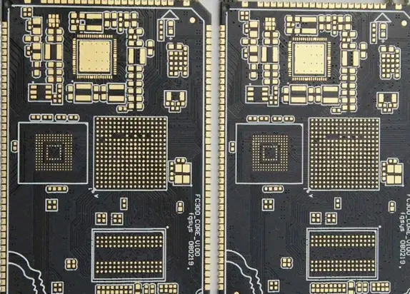
1. The Foundation: Land Pattern and Pad Design
The PCB land pattern is the literal foundation of your BGA component. Getting this right is non-negotiable.
Pad Size and Shape: Use Non-Solder Mask Defined (NSMD) pads. NSMD pads have the copper defined smaller than the solder mask opening, which allows the solder mask to anchor the pad and provides a superior mechanical connection. The recommended pad diameter is typically 80% to 90% of the BGA ball pitch.
For 1.0mm pitch: A 0.25mm (10mil) drill diameter with a 0.36mm (14mil) capture pad is a good starting point.
For 0.8mm pitch: Use a 0.3mm (12mil) pad.
For 0.5mm pitch: A 0.23mm (9mil) pad is common.
Always consult the manufacturer's datasheet for their recommended land pattern.
Solder Mask Control: The solder mask dam between pads must be precise. A dam that is too small can lead to solder bridging between balls. A dam that is too large can encroach on the pad, reducing the available solderable area. Ensure a clean, defined web between all BGA pads.
2. The Critical Decision: Via-in-Pad vs. Dog Bone Routing
How you escape the dense array of pins under a BGA is a pivotal design choice.
Via-in-Pad (VIPPO): This technique places a via directly in the BGA pad, which is then filled and capped with copper.
Pros: Maximizes routing density, allows for smaller component pitch, and provides an excellent thermal path.
Cons: Significantly increases fabrication cost. Requires strict process control to prevent solder wicking into the via during reflow, which can cause solder joint voids.
Dog Bone (Fanout) Routing: This is the traditional method, where a short trace connects the BGA pad to a via located outside the pad area.
Pros: Lower cost, easier to manufacture and inspect, less risk of solder wicking.
Cons: Consumes more real estate on outer layers, limiting routing density. Not suitable for the finest-pitch BGAs.
Recommendation: Use dog bone fanouts for pitches of 0.8mm and larger. For 0.5mm and finer pitches, Via-in-Pad is often the only viable option, and the associated cost must be accepted.
3. Effective PCB Routing Strategies Under a BGA
4. Designing for Thermal Management and Power Integrity
BGAs, especially processors and FPGAs, generate significant heat and demand clean power.
Thermal Relief: Connect power and ground planes to vias using thermal relief spokes. This prevents the plane from acting as a heat sink during soldering, which can cause cold solder joints.
Solid Thermal Connection: For thermal pads (large exposed pads on the bottom of the BGA), use a pattern of vias to connect directly to an internal ground plane. This acts as a primary heat dissipation path. Fill these vias with thermally conductive epoxy for best results.
Decoupling Capacitors: Place decoupling capacitors as close as possible to the BGA's power pins. Use a mix of bulk and small-value capacitors to filter a wide range of noise. The shortest possible loop inductance is critical.
5. Incorporating Design for Manufacturing (DFM) and Testing (DFT)
A design is only successful if it can be built and tested reliably.
Stencil Aperture Design: Work with your SMT assembly house to design the solder paste stencil. Slightly reducing the aperture size for BGA pads (e.g., 1:1 ratio or a slight reduction to 95%) can help prevent solder bridging.
Fiducials and Tooling Holes: Provide global and local fiducials. Local fiducials, placed near the BGA, are crucial for precise placement, especially for fine-pitch components.
Test Point Access: During the fanout and routing phase, ensure that critical signals are brought out to accessible test points for in-circuit testing (ICT). Trying to probe a 0.5mm BGA ball is impossible.
Conclusion: A Checklist for Success
To ensure a high-yield, reliable BGA design, use this final checklist:
Confirmed land pattern with NSMD pads.
Selected appropriate fanout strategy (Dog Bone vs. Via-in-Pad).
Escaped all signals using a logical, layered approach.
Implemented proper thermal management (thermal vias, reliefs).
Placed decoupling capacitors optimally.
Validated design with your PCB fabricator and assembly house.
By adhering to these BGA PCB design guidelines, you move beyond simply making a connection. You build a robust, manufacturable, and reliable foundation for your most critical components, saving time and cost while delivering a superior product.