Printed Circuit Board (PCB) edge connectors, also known as card edge connectors, offer a simple, cost-effective, and reliable way to connect a daughter board to a mother board. Unlike separate connectors that are soldered onto the PCB, the connector itself is formed by a portion of the PCB, which is plated with exposed contacts (often called "gold fingers"). This design eliminates the need for a separate component, saving cost and space.
However, the success of this elegant solution hinges entirely on one critical factor: dimensional accuracy. A mismatch of even a few tenths of a millimeter can lead to poor electrical contact, mechanical instability, or complete failure to mate. In this comprehensive guide, we will break down the essential dimensions you must consider when designing a PCB for an edge connector.
The Critical Trio: Thickness, Pitch, and Length
When discussing key dimensions for PCB edge connectors, three parameters are paramount. They form the foundation of the interface between your PCB and the mating connector.
1. PCB Thickness (T)
This is arguably the most crucial dimension. The thickness of your PCB directly determines the size and type of the mating connector it will fit into.
Standard Range: The most common PCB thickness is 1.6mm (approximately 0.063 inches). Mating connectors are widely available for this standard.
Other Common Thicknesses: Thinner boards, such as 0.8mm and 1.0mm, are also frequently used, especially in compact consumer electronics. Thicker boards (e.g., 2.0mm, 2.4mm) may be used for high-power or high-durability applications.
Why it Matters: The mating connector is designed with a specific slot width to create a precise interference fit (friction fit) with the PCB. If the PCB is too thick, it will not insert or may damage the connector. If it's too thin, the connection will be loose, leading to signal interruption and arcing.
Actionable Tip: Always confirm the required PCB thickness with the datasheet of your chosen mating connector before starting your PCB layout.
2. Contact Pitch (P)
Pitch refers to the center-to-center distance between adjacent contacts (gold fingers) on the PCB. It defines the density of the connections you can achieve.
Standard Pitches: The most common pitch for standard board-to-board applications is 2.54mm (0.100 inches) and 2.0mm (0.079 inches). These are robust and widely supported.
Fine-Pitch Connectors: For high-density applications, finer pitches like 1.27mm (0.050 inches) and even 0.8mm or 0.635mm are available. These require higher manufacturing precision.
Implication: A finer pitch allows for more signals in a smaller space but can increase cost and requires stricter control over PCB fabrication and gold finger plating.
3. Contact Length and Engagement Depth (L)
This dimension refers to the length of the plated gold finger along the edge of the board. It must be long enough to ensure a secure and stable electrical connection once fully inserted into the mating connector.
Typical Length: Engagement lengths can vary but typically range from 5mm to 10mm or more.
Design Consideration: The contact length must be designed in conjunction with the mating connector's contact spring length. A longer engagement provides better stability and current-carrying capacity. You must ensure that the gold finger plating extends far enough into the connector to make reliable contact but does not extend so far that it interferes with the PCB's mounting or other components.
Other Essential Dimensions to Specify
Beyond the big three, several other dimensions are critical for a successful design.
4. Contact Width and Spacing (W & S)
The width of each individual gold finger and the space between them must be clearly defined. These are typically derived from the pitch (P = W + S).
Standard Practice: Often, the contact width and spacing are equal. For example, in a 2.54mm pitch, a common pattern is a 1.27mm wide finger with a 1.27mm gap.
Beveling (Chamfer): The leading edge of the PCB that inserts into the connector must be beveled. A typical bevel is 30° to 45°. This chamfer guides the PCB into the slot and prevents damage to the delicate spring contacts inside the mating connector.
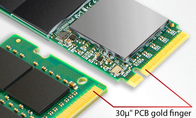
5. Gold Finger Plating Thickness
While not a "macro" dimension, the thickness and type of plating are electrically critical.
Hard Gold: Edge connectors almost always use "hard gold" (a gold-cobalt or gold-nickel alloy) over a nickel barrier layer. Hard gold is wear-resistant, capable of withstanding repeated insertions.
Thickness: A common specification is 15-30 microinches (0.38 - 0.76 µm) of gold over 50-100 microinches of nickel. For high-reliability or frequently mating connectors, a thicker gold plating (e.g., 30 µin) is recommended.
6. Overall PCB Profile and Slotting
In some cases, the edge connector area is not a simple rectangle. Designers may include notches, slots, or cutouts to provide polarization—ensuring the board can only be inserted in the correct orientation. The position and size of these polarization features are key dimensions that must be precisely controlled.
Practical Design Checklist
Before you send your PCB for fabrication, ask yourself:
Mating Connector Selected? Have I chosen a specific mating connector and studied its datasheet for all required PCB dimensions?
Thickness Correct? Is the PCB stack-up defined to achieve the final thickness (T) required by the connector?
Pitch Defined? Are the contact pitch (P), width (W), and spacing (S) clearly defined in my PCB CAD software?
Bevel Present? Have I specified a bevel on the insertion edge in my fabrication drawings?
Plating Specified? Have I clearly called out "Hard Gold Plating" on the fingers and specified the thickness in my notes to the manufacturer?
Polarization? Have I included and correctly dimensioned any polarization notches if needed?
Conclusion
Understanding the key dimensions for a PCB edge connector is not just an academic exercise—it is fundamental to creating a functional and reliable product. By meticulously defining and controlling the PCB thickness, contact pitch, contact length, bevel, and plating specifications, you can avoid costly redesigns and manufacturing errors. Always begin with the mating connector's datasheet and work backward to define your PCB's edge connector requirements. This proactive approach ensures a perfect, reliable fit every time.