What Is THT Technology
|
<Aspect</ |
<Through-Hole Technology (THT)</ |
<Surface-Mount Technology (SMT)</ |
|
Component Placement |
Leads inserted through PCB holes; soldered on the opposite side |
Components mounted directly on PCB surface; soldered to top/bottom pads |
|
Mechanical Stability |
Exceptional—resistant to vibration and physical stress |
Moderate—relies on surface solder joints, more prone to damage from impact |
|
Power Handling |
High—ideal for high-current, high-voltage components |
Lower—suited for low-to-medium power applications |
|
PCB Density |
Lower—requires drilled holes, limiting component placement density |
Higher—components are smaller and can be placed on both sides without holes |
|
<Aspect</ |
<Through-Hole Technology (THT)</ |
<Surface-Mount Technology (SMT)</ |
|
Assembly Speed |
Slower—manual or semi-automated processes for insertion |
Faster—fully automated pick-and-place machines for high-volume production |
|
Cost (High-Volume) |
Higher—labor-intensive insertion and drilling processes |
Lower—automation reduces labor costs for mass production |
|
Repair and Rework |
Easier—components can be removed and replaced manually |
More complex—requires specialized tools (e.g., hot air stations) to avoid PCB damage |
|
Thermal Performance |
Better heat dissipation due to through-hole pathways |
Inferior—surface joints retain more heat, requiring thermal management solutions |
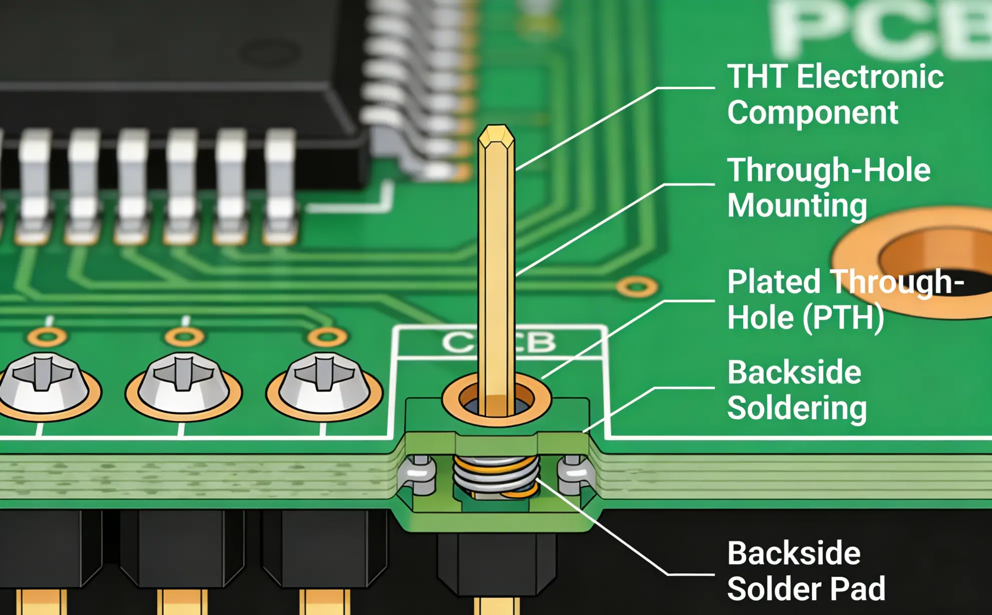
THT PCB Design Guidelines
Designing a THT PCB requires careful consideration of hole placement, pad dimensions, and component spacing to ensure manufacturability and performance. Key design tips include:
· Hole Sizing: Drill holes should be 0.1–0.2 mm larger than component leads to allow easy insertion while maintaining a tight fit for soldering. Standard lead diameters (e.g., 0.5 mm, 0.8 mm) dictate corresponding hole sizes.
· Pad Design: THT pads are typically circular, butoval-shaped pads are acceptable for components subjected to directional stress (e.g., connectors) or when space is limited. Oval pads provide increased solder joint area and better mechanical stability.
· Component Spacing: Maintain a minimum distance of 1.5–2 mm between adjacent holes and components to prevent solder bridging and ensure access for soldering tools.
· Trace Width: For high-power THT components, use wider traces (≥1 mm for 1A current) to minimize resistance and heat buildup.
· High-Density Interconnect (HDI) for THT: Achieving HDI in THT PCBs requires optimizing hole patterns, using smaller drill sizes (down to 0.3 mm), and integrating blind/buried vias where possible. Additionally, double-sided THT assembly (components on both PCB sides) maximizes density without sacrificing performance.
THT PCB Production Cycle
The production cycle for THT PCBs varies based on order volume, design complexity, and manufacturing processes, but typically follows this timeline:
1. PCB Fabrication (3–7 days): Includes substrate cutting, drilling, copper plating, solder mask application, and silkscreen printing. Drilling through-holes is a critical step that adds 1–2 days compared to SMT-only PCBs.
2. Component Sourcing (1–5 days): Procuring THT components (resistors, capacitors, connectors, etc.) based on the bill of materials (BOM).
3. Assembly (1–3 days): Manual or semi-automated insertion of components into drilled holes, followed by wave soldering (the primary soldering method for THT) to secure leads to pads.
4. Quality Inspection (0.5–1 day): Visual inspection, electrical testing, and solder joint verification to ensure compliance with industry standards (e.g., IPC-A-610).
5. Final Testing and Packaging (0.5–1 day): Functional testing of the assembled PCB and packaging for shipment.
Overall, the total production cycle for THT PCBs ranges from5–17 days, with low-volume orders (≤100 units) taking 5–10 days and high-volume or complex designs requiring 10–17 days.
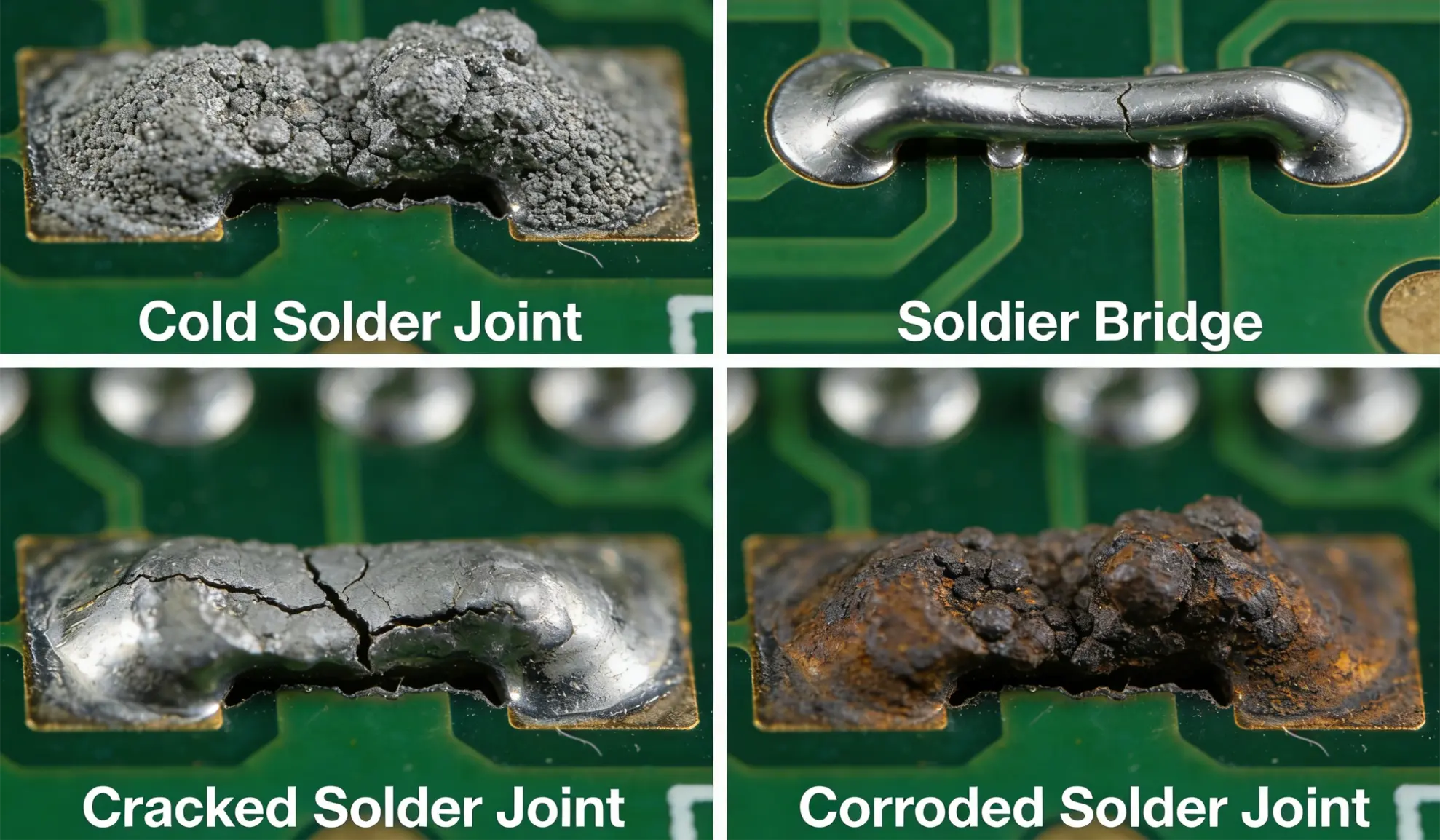
Common Causes of THT Solder Joint Failure
THT solder joints are highly reliable, but failure can occur due to design flaws, manufacturing errors, or environmental factors. Common causes include:
· Poor Soldering Technique: Insufficient solder coverage, cold solder joints (due to inadequate heat), or solder bridging (excess solder connecting adjacent pads) can lead to electrical discontinuity or short circuits.
· Thermal Cycling Stress: Repeated exposure to temperature fluctuations (e.g., in automotive or industrial settings) causes the PCB substrate and component leads to expand and contract at different rates, leading to solder joint cracking.
· Mechanical Damage: Vibrations, impact, or improper handling during assembly/installation can weaken or break through-hole solder joints.
· Corrosion: Moisture, humidity, or exposure to chemicals (e.g., in harsh environments) can corrode solder joints, reducing conductivity and mechanical strength.
· Component Lead Issues: Bent, oxidized, or contaminated leads prevent proper solder adhesion, resulting in weak joints.
THT PCB Quality Inspection Methods
Ensuring the quality of THT PCBs requires a combination of visual, electrical, and mechanical testing. Key inspection techniques include:
· Visual Inspection: Manual or automated optical inspection (AOI) to check for solder joint defects (e.g., cold solder, bridging, insufficient solder), component misalignment, and damaged leads.
· Electrical Testing: Continuity testing (to verify electrical connections), insulation resistance testing (to detect shorts), and functional testing (to ensure the PCB operates as intended).
· Mechanical Testing: Pull testing to measure the tensile strength of solder joints and verify resistance to physical stress.
· SEM-EDS Analysis: Scanning Electron Microscopy (SEM) combined with Energy-Dispersive X-ray Spectroscopy (EDS) is used for failure analysis. SEM provides high-resolution images of solder joint microstructures (e.g., cracks, voids), while EDS identifies elemental composition (e.g., solder alloy purity, contamination) to pinpoint failure causes.
Selecting Solder Paste and Flux for Through-Hole Reflow (THR)
Through-Hole Reflow (THR) is a hybrid process that combines THT component insertion with reflow soldering (typically used for SMT). Choosing the right solder paste and flux is critical for successful THR:
· Solder Paste Selection: Opt for a paste with ahigh melting point alloy (e.g., Sn63/Pb37, Sn96.5/Ag3.0/Cu0.5) compatible with THT component lead materials (copper, brass). The paste should have good wetting properties to ensure full coverage of through-holes and pads. For high-reliability applications, lead-free solder pastes (compliant with RoHS standards) are preferred.
· Flux Selection: Use ano-clean or water-soluble flux with strong activators to remove oxidation from component leads and PCB pads. The flux should have a long activity window to withstand the reflow temperature profile (typically 210–230°C for lead-free solder) and leave minimal residue to avoid corrosion. For THR, flux with good capillary action is essential to draw solder paste through the hole and form a robust joint.
THT PCB Tin Plating Requirements
Tin plating is a critical surface finish for THT PCBs, as it enhances solderability, prevents copper oxidation, and improves electrical conductivity. Key requirements include:
· Plating Thickness: A minimum tin thickness of 0.8–1.2 μm is recommended to ensure long-term solderability and corrosion resistance. Thicker plating (1.5–2.0 μm) is suitable for harsh environments.
· Plating Uniformity: Tin should be evenly distributed across all through-holes and pads to avoid thin spots that can lead to oxidation or poor solder adhesion.
· Adhesion: The tin layer must adhere firmly to the underlying copper to prevent peeling or flaking during assembly or operation.
· RoHS Compliance: For eco-friendly applications, use lead-free tin plating (e.g., pure tin, tin-silver alloy) that meets RoHS standards.
Protecting THT Components on SMT Production Lines
Integrating THT components into SMT production lines requires careful measures to avoid damage, as SMT processes (e.g., reflow soldering, automated handling) are optimized for surface-mount parts:
· Component Orientation: Secure THT components with fixtures or tape to prevent movement during SMT pick-and-place or reflow processes.
· Temperature Control: Adjust reflow oven profiles to lower peak temperatures (if possible) or use heat shields for heat-sensitive THT components (e.g., electrolytic capacitors) to avoid thermal damage.
· Handling Equipment: Use gentle handling systems (e.g., soft grippers) to prevent bending or breaking THT leads during automated transport.
· Separate Processing Stages: Perform THT insertion and wave soldering as a separate post-SMT process to avoid exposing THT components to SMT-specific stresses (e.g., high-speed placement).
THT PCB Material Selection and Supplier Insights
Selecting the right PCB material for THT applications depends on factors like operating temperature, power requirements, and environmental conditions. Common materials include:
· FR-4: The most widely used material for THT PCBs, offering good mechanical strength, electrical insulation, and cost-effectiveness. Suitable for general-purpose electronics (e.g., industrial controls, consumer devices).
· High-Temperature Materials (e.g., FR-5, Polyimide): Ideal for high-power THT applications or environments with elevated temperatures (e.g., automotive engine bays, aerospace systems). These materials withstand higher heat without degrading.
· Rigid-Flex PCBs: For THT components in compact or curved designs (e.g., wearable electronics, medical devices), rigid-flex materials combine the durability of rigid PCBs with the flexibility of flexible substrates.
Top THT PCB Material Suppliers
· Isola Group: Offers high-performance FR-4 and specialty materials for industrial, automotive, and aerospace THT applications.
· Rogers Corporation: Provides advanced materials (e.g., RO4000 series) for high-frequency, high-power THT PCBs.
· Taiyo Ink Co., Ltd.: Supplies solder masks and PCB substrates optimized for THT assembly.
· Kingboard Holdings: A leading manufacturer of FR-4 and lead-free compatible materials for cost-sensitive THT projects.
When selecting suppliers, prioritize those with ISO 9001 and IPC-6012 certifications to ensure material quality and compliance with industry standards.