Technical Specifications and Manufacturing of an 8-Layer HDI PCB for Mobile Phone Main Boards
The demand for more powerful, compact, and feature-rich mobile devices drives continuous innovation in printed circuit board (PCB) technology. High-Density Interconnect (HDI) PCBs are at the core of this evolution, enabling the complex circuitry required for modern smartphones. This article details the technical specifications and manufacturing considerations for a standard 8-Layer HDI PCB used in a mobile phone main board (motherboard).
Key Specifications Overview
"This PCB is engineered to meet the rigorous space, performance, and reliability standards of the mobile industry. Below is a breakdown of its critical parameters:
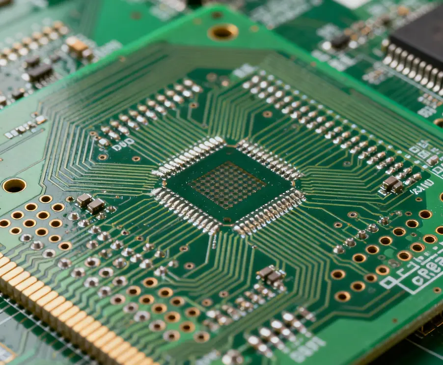
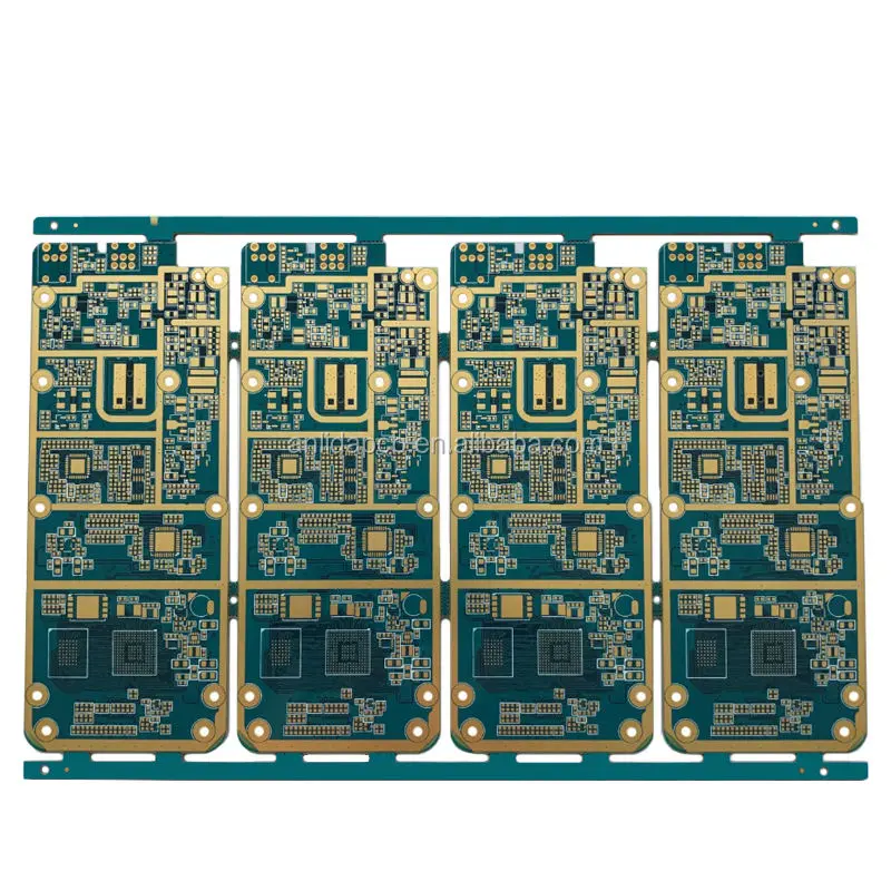
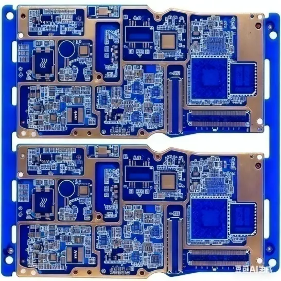
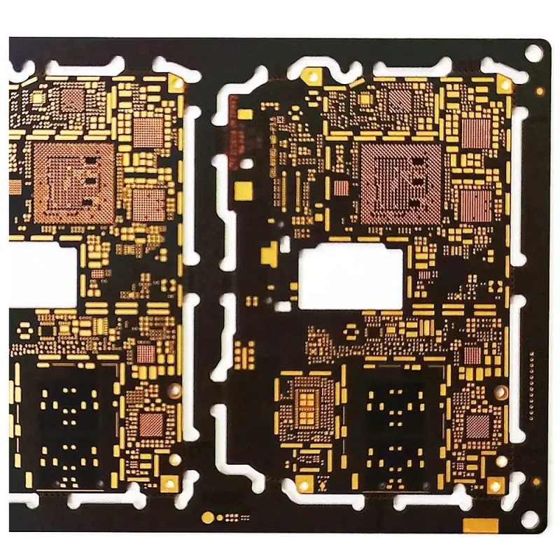
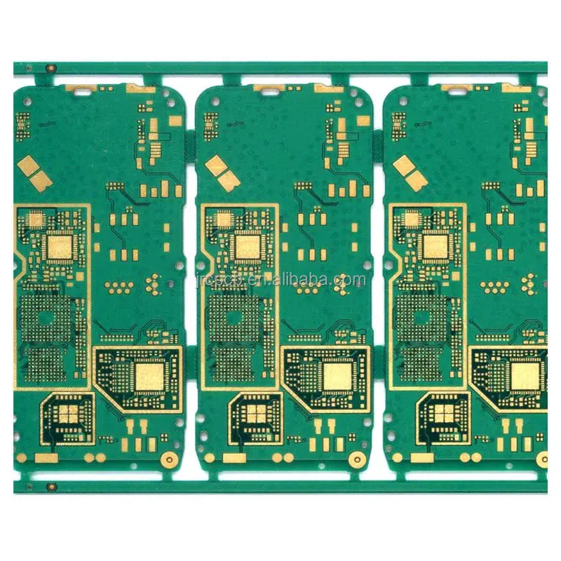
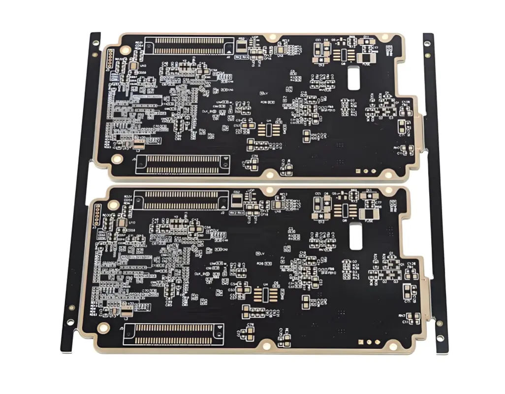
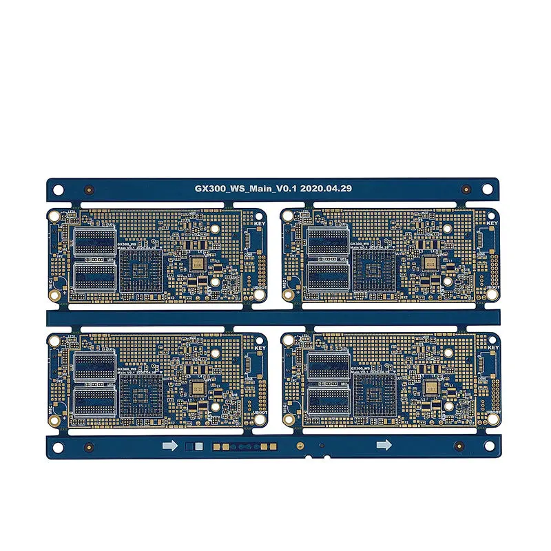
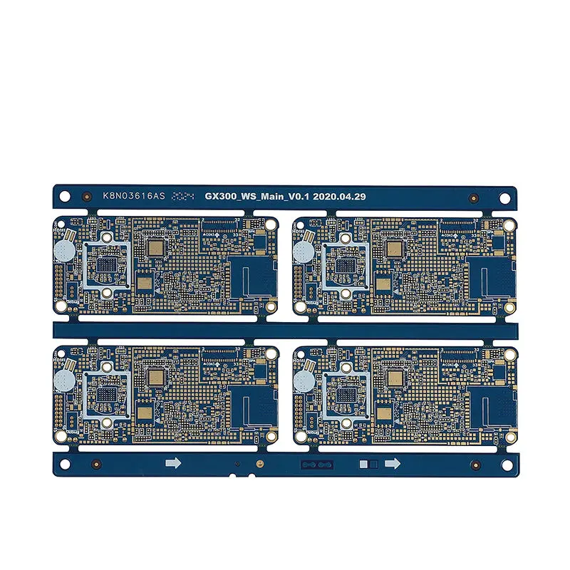
1、Model & Construction: The board is designated as an 8L 2+N+2 Mobile Main Board. The ""2+N+2"" stack-up indicates a core (N) laminated between two sets of sequential build-up layers. This is a classic HDI structure that allows for higher component density and improved signal integrity compared to standard PCBs.
2、Base Material: The substrate used is standard FR-4, a flame-retardant epoxy laminate that offers an excellent balance of mechanical strength, electrical insulation, and cost-effectiveness for high-volume consumer electronics.
3、Finished Board Thickness: The final product has a compact thickness of 1.0mm. This slim profile is essential for achieving the sleek form factors demanded by today's mobile phones.
4、Copper Thickness: The finished copper weight is 1 oz per square foot, which is typical for controlling impedance and carrying the required current for smartphone applications.
5、Solder Mask & Silkscreen: The board is available with either Green or White solder mask. The surface finish is Immersion Gold (ENIG), which provides a flat, solderable surface with excellent oxidation resistance, ideal for fine-pitch components.
6、Fabrication Tolerances: The board features advanced manufacturing capabilities:
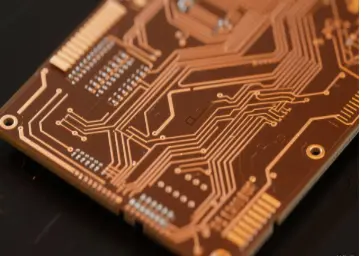
6-1、Min. Trace/Space: 3.5 mil / 3.5 mil. This fine line geometry is crucial for routing a high number of connections in a confined space.
6-2、Min. Hole Sizes: It utilizes both mechanical drilling (0.2mm) and laser drilling for microvias (0.1mm). Laser-drilled microvias are a hallmark of HDI technology, allowing for dense interconnections between layers."
Manufacturing and Design Significance
The combination of an 8-layer stack-up and HDI technology is pivotal for mobile main boards. It provides sufficient layers for segregating power, ground, and high-speed signal lines (such as those for the processor and memory), which minimizes electromagnetic interference (EMI) and crosstalk.
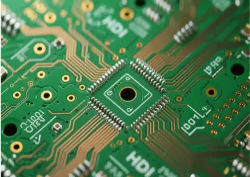
The use of laser microvias (0.1mm) is particularly significant. These small vias enable more direct routing paths, reduce layer count for a given functionality, and free up valuable real estate on the board surface for component placement. The ENIG surface finish ensures reliable solder joints for Ball Grid Array (BGA) packages and other miniature components commonly found on mobile motherboards.
Primary Application
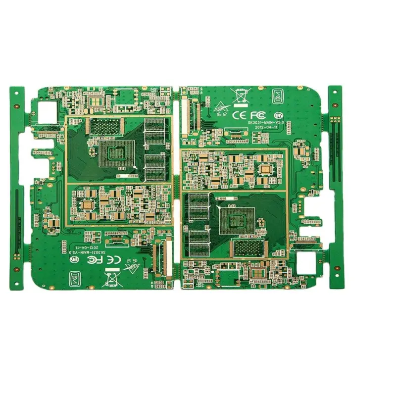
This specific set of specifications is predominantly used in the manufacturing of the main logic board (MLB) or motherboard for mobile phones. This board acts as the central nervous system of the device, hosting the application processor, memory, RF modules, and power management ICs.
"The detailed specifications of this 8-Layer HDI PCB underscore the precision engineering required in modern consumer electronics. Parameters like the 2+N+2 build-up, 3.5 mil trace width, and 0.1mm laser microvias are not arbitrary; they are carefully chosen to balance performance, size, and manufacturability. For engineers and procurement specialists, understanding these specs is key to selecting the right PCB partner for high-performance, compact electronic devices.
"
Product Designation: 8-Layer 2+N+2 Mobile Main Board PCB
Base Material: FR-4
Layer Construction: 8-Layer HDI (High-Density Interconnect) with 2+N+2 stack-up
Board Thickness: 1.0 mm (finished)
Copper Weight: 1 oz (finished)
Solder Mask Color Options: Green or White
Surface Finish: Immersion Gold (ENIG)
Minimum Line Width / Spacing: 3.5 mil / 3.5 mil
Minimum Drilled Hole Sizes:
Mechanical Drill: 0.2 mm
Laser Micro-via: 0.1 mm
Primary Application: Mobile Device Main Logic Board (Motherboard)