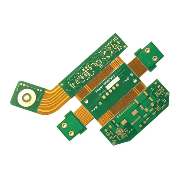
Rigid-flex PCBs represent a pinnacle of innovation in electronic interconnect solutions, seamlessly integrating the durability of rigid boards with the flexibility of dynamic circuits. This article provides a detailed technical examination of an 8-layer rigid-flex PCB (R-FPCB), breaking down its key manufacturing specifications and ideal use cases for engineers and procurement specialists.
Core Construction and Material Selection
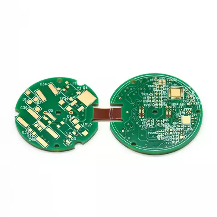
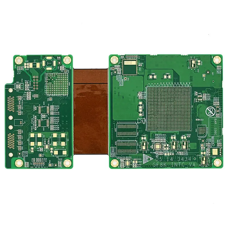
"The model in question features an 8-layer rigid-flex construction, a sophisticated stack-up designed for complex, high-density applications. The core material set is a combination of FR-4 for the rigid sections and Polyimide (PI) for the flexible layers.
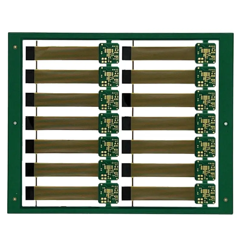
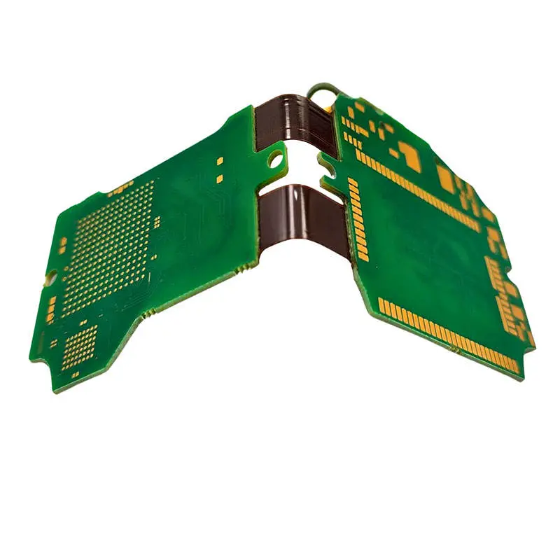
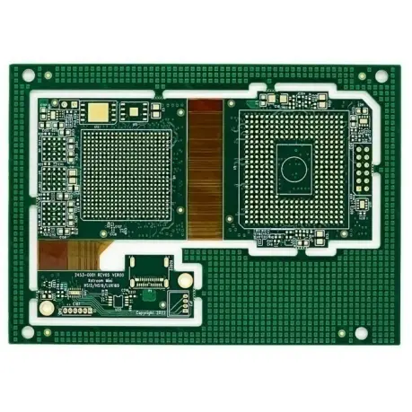
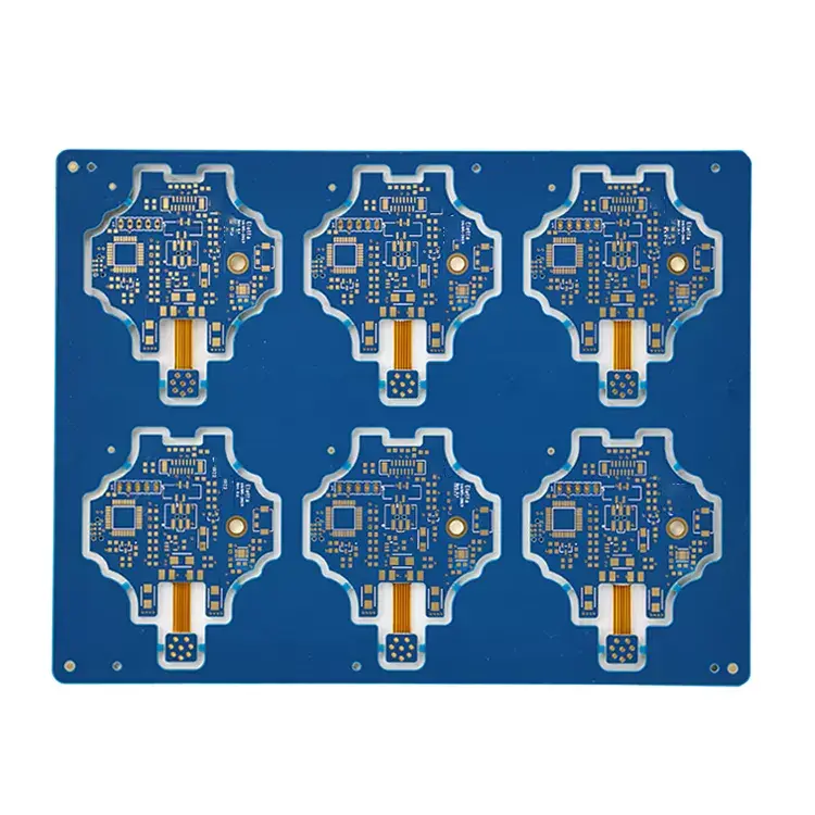
1、Stack-up Configuration: The board employs a balanced 4-layer FR4 + 4-layer Flex architecture. This configuration typically allows for two rigid sections connected by a flexible ribbon, enabling a reliable, three-dimensional assembly that eliminates the need for connectors and cables between board parts.
2、Material Rationale: FR-4 provides excellent structural rigidity and cost-effectiveness for component mounting, while Polyimide offers superior thermal stability, flexibility, and resistance to cracking under repeated bending stresses."
Critical Manufacturing Specifications and Tolerances
"Precision manufacturing is paramount for the functionality of rigid-flex boards. The following specifications highlight the capabilities required for production.
1、Finished Thickness: The board features a differentiated thickness profile. The flexible circuit area is 0.2mm thick, ensuring pliability, while the rigid sections measure 0.8mm, providing the necessary structural support. This differential is achieved through precise layer stacking and lamination processes.
2、Copper Thickness: A standard 1 oz (approximately 35µm) copper weight is specified for all layers. This offers an optimal balance for current-carrying capacity and fine-line etching capabilities.
3、Minimum Trace/Space: The design rules permit a minimum of 5 mil (0.127mm) for both trace width and spacing. This level of precision is essential for routing high-density interconnect (HDI) designs commonly found in advanced electronics.
4、Drilling and Hole Size: The specified minimum mechanical hole size is 0.2mm. While this indicates capability for very small vias, it's important to note that laser drilling is often used for microvias in HDI rigid-flex designs, offering even greater density.
5、Surface Finish and Solder Mask: The board utilizes Immersion Gold (ENIG) as its surface treatment. ENIG provides a flat, solderable surface with excellent oxidation resistance, which is critical for the reliable soldering of fine-pitch components. The solder mask is available in standard green or white, with white often preferred for applications requiring enhanced LED reflectivity or visual inspection clarity."
Primary Application: Equipment Switching PCBs
"The designated application for this 8-layer rigid-flex PCB is in equipment switching systems, such as network switches, routers, and data center infrastructure. This application is a perfect match for the board's capabilities for several reasons:
1、Space Savings: By folding the circuitry in three dimensions, rigid-flex designs dramatically reduce the overall footprint and weight of the assembly.
2、Enhanced Reliability: The elimination of board-to-board connectors—a common point of failure—significantly improves the long-term reliability and signal integrity of the system.
3、High-Density Integration: The 8-layer count allows for complex routing necessary for high-speed data buses and control signals within switching equipment."
This 8-layer rigid-flex PCB exemplifies a sophisticated interconnect solution tailored for demanding electronic environments. Its specific material composition, precise manufacturing tolerances, and robust construction make it an ideal choice for next-generation equipment switching PCBs and other advanced applications where reliability, space constraints, and performance are non-negotiable. Understanding these specifications is the first step in selecting the right rigid-flex partner for your project.
Configuration: 8-Layer Rigid-Flex Construction
Base Material: FR4 and Polyimide (PI) Combination
Stack-up: 4-Layer FR4 Rigid Sections + 4-Layer Flex Circuit
Finished Thickness: 0.2mm (Flex Region) + 0.8mm (Rigid Region)
Copper Weight: 1 oz (Approx. 35µm)
Solder Mask: Green or White
Surface Finish: Immersion Gold (ENIG)
Minimum Trace/Spacing: 5/5 mil (Inner/Outer Layers)
Minimum Drill Size: 0.2mm (Mechanical Holes)
Application: Primary Use in Equipment Switching PCBs (e.g., network switches, routers)

")
")