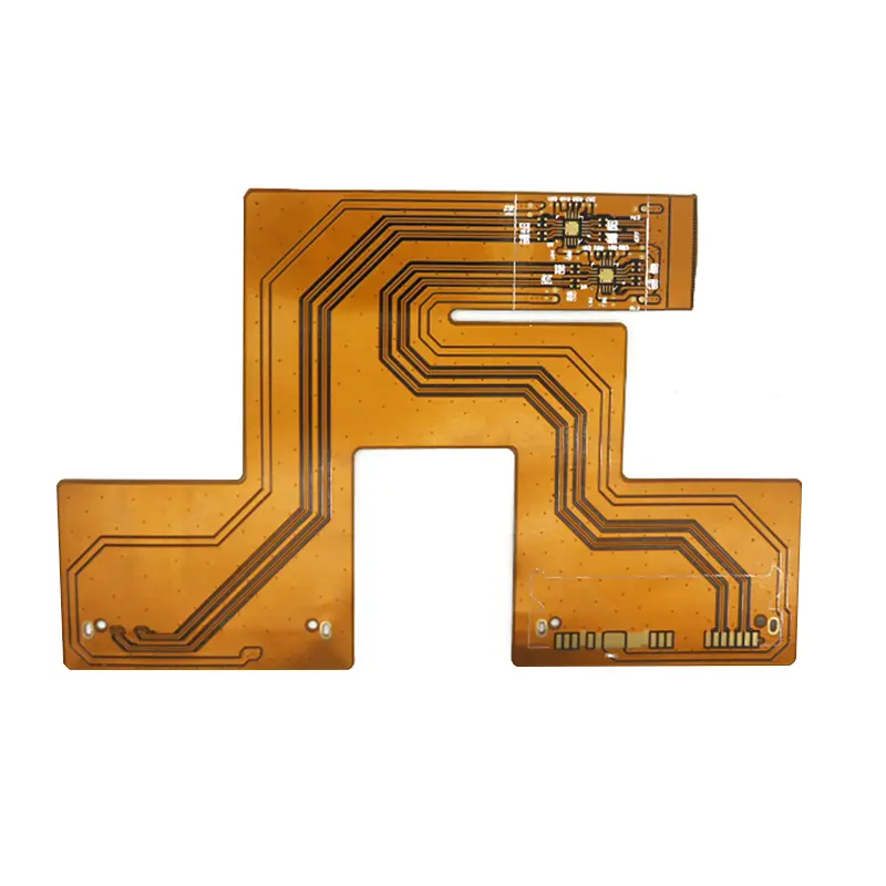
Technical Specifications for Advanced Flexible Printed Circuit Board (FPCB) Manufacturing
In the rapidly evolving electronics industry, the demand for high-density, high-reliability Flexible Printed Circuits (FPCs) is greater than ever. Manufacturers require a partner capable of delivering precision, versatility, and rapid turnaround. This technical overview details the advanced manufacturing capabilities for producing high-performance FPCBs that meet these stringent demands.
1. Core Mechanical & Dimensional Specifications
This set of parameters defines the foundational physical limits of our standard FPCB production process, ensuring robust and reliable board construction.
"Copper Thickness: Standard offerings of 0.5 oz and 1.0 oz, providing a balance of current carrying capacity and flexibility.
1、Supply Type: Comprehensive OEM and ODM Services, allowing for complete customization from design to finished product.
2、Minimum Laser Drilled Hole Size: 0.1 mm, enabling high-density interconnects (HDI) for complex designs.
3、Minimum Trace/Space (Line Width/Spacing): 2.5/2.5 mil, a standard for reliable signal integrity in most flexible applications.
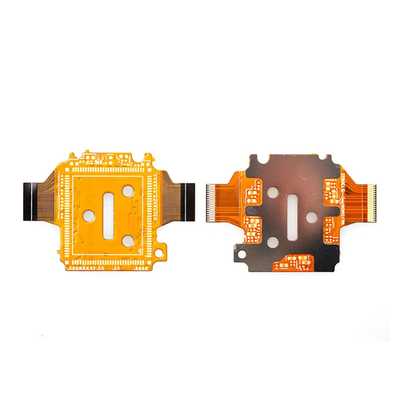
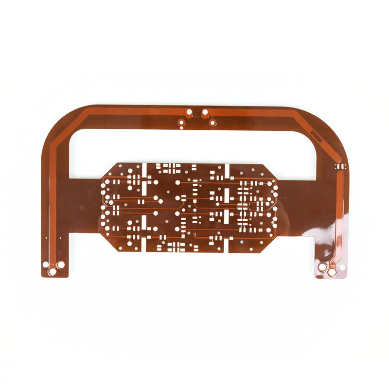
4、Maximum Layer Count: Support for up to 12 layers, facilitating sophisticated multi-layer circuit designs in a flexible format.
5、Board Thickness Range: A wide range from 0.06 mm to 0.5 mm, accommodating applications requiring extreme flexibility or added rigidity.
6、Maximum Finished Panel Size: Large-format capability of 9 x 98 inches, ideal for applications like flexible displays or long, intricate connectors.
7、Minimum Routing (Outline) Tolerance: A tight tolerance of ±0.05 mm, ensuring precise dimensional accuracy for perfect fitment.
8、Stiffener Materials: A variety of options including FR4, PI (Polyimide), PET, SUS (Stainless Steel), and PSA (Pressure-Sensitive Adhesive) to provide localized rigidity for component mounting and connector stability."
2. Advanced High-Density Interconnect (HDI) Capabilities
"For projects demanding the highest level of precision, our advanced HDI processes push the boundaries of miniaturization.
1、Ultra-Fine-Pitch Fabrication:
1-1、Minimum Line Width & Spacing: 0.05 mm
1-2、Minimum Aperture Size: 0.05 mm
This ultra-fine capability is essential for modern, compact devices such as wearables, medical sensors, and advanced camera modules.
3、Extended Layer Capacity: Capability to produce FPCBs with up to 16 layers, supporting the most complex circuit architectures.
4、Surface Finish: Standard use of OSP (Organic Solderability Preservative), a lead-free finish that provides a flat, reliable surface for soldering components.
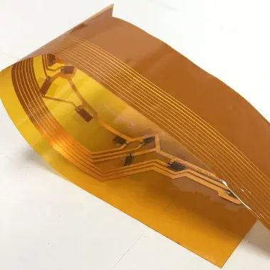
5、Base Laminate: Utilization of high-quality Paper Phenolic Copper-Clad Laminate (CCL) as a standard base material, known for its excellent electrical insulation and mechanical properties.
6、Quality Assurance: 100% Electrical Testing is performed on every board to guarantee functionality and reliability, catching any potential defects like opens or shorts."
Service & Customization Options
"We understand that flexibility extends beyond the product to the service model itself.
Silkscreen Color Options: Multiple colors available (Black, White, Yellow, Red, Blue) for clear component designation and branding.
Minimum Order Quantity (MOQ): An exceptionally low MOQ of 1 Piece, ideal for prototyping and low-volume production runs without excessive cost.
Delivery Lead Time: Competitive standard lead times of 10 to 15 days, enabling faster time-to-market for your products."
"These comprehensive specifications demonstrate a mature and capable FPCB manufacturing process. From standard multi-layer boards to advanced HDI designs, the combination of precise tolerances, a wide range of materials, and a flexible service model makes this an ideal solution for engineers and procurement specialists seeking a reliable manufacturing partner for their next-generation electronic devices.
For specific project requirements, including custom copper thickness options (1/4 oz, 1/3 oz, 2/3 oz, 1/2 oz), please contact our engineering team for a consultation."
Copper Thickness: 0.5 oz / 1 oz
Minimum Hole Size: 0.1 mm
Minimum Trace/Space: 2.5 / 2.5 mil
Maximum Layer Count: 16 Layers
Board Thickness: 0.06 - 0.5 mm
Maximum Finished Board Size: 9 x 98 inches
Minimum Routing Tolerance: ±0.05 mm
Minimum Mechanical Drilling Size: 0.1 mm
Stiffener Types: FR4, PI, PET, SUS, PSA