Advanced PCB Manufacturing: Technical Specifications and Engineering Capabilities
Modern electronics manufacturing demands precision engineering and rigorous quality control. This overview details the key technical specifications available in contemporary PCB fabrication services, highlighting capabilities that meet stringent industry requirements for various applications.
Core Material Specifications and Construction
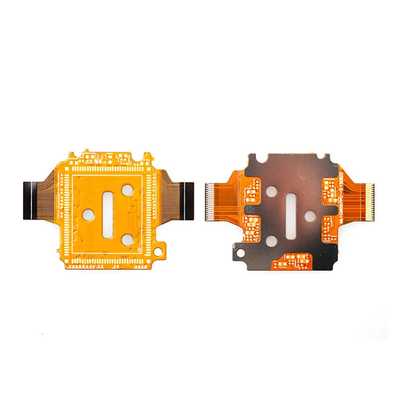
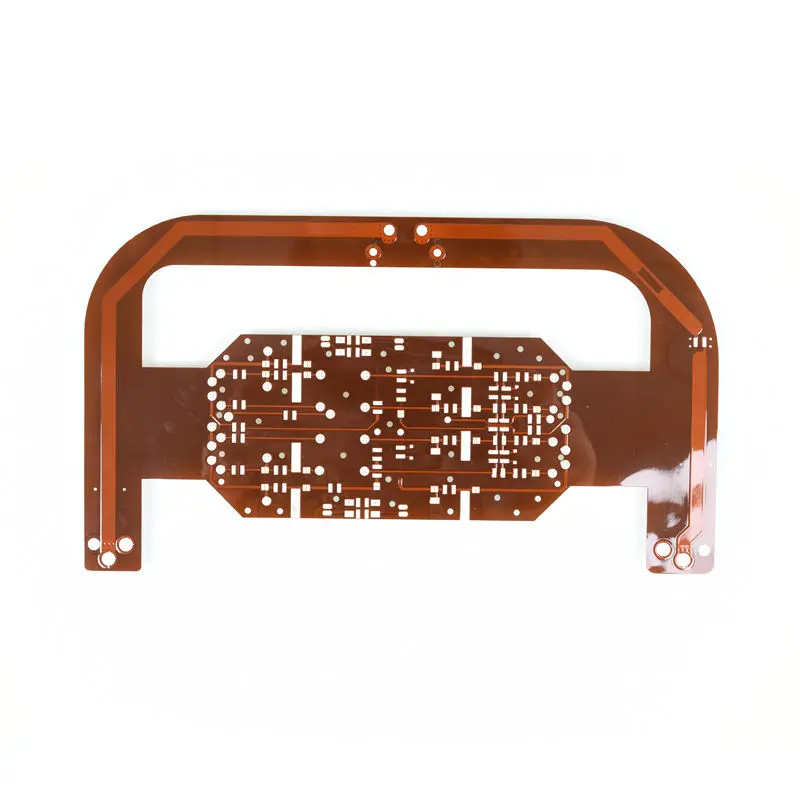
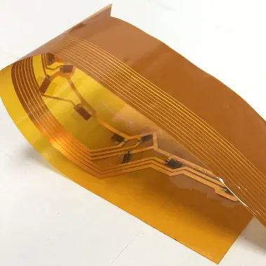
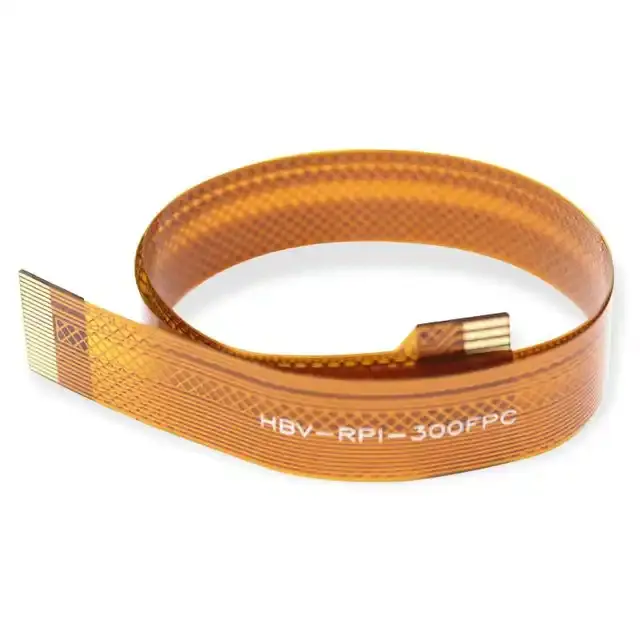
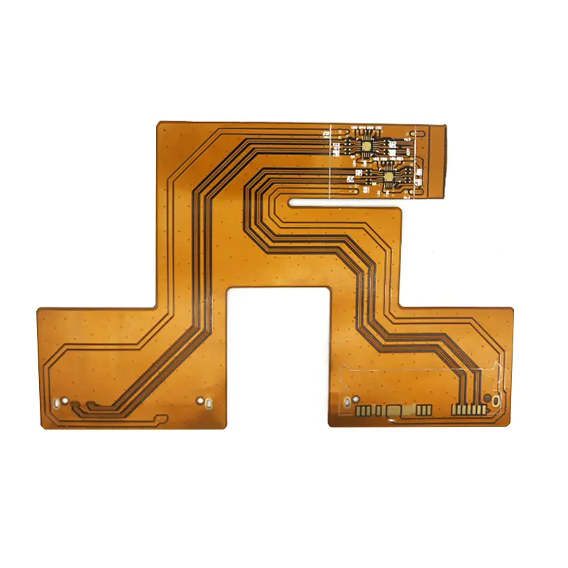
PCB fabrication begins with core material selection. Standard offerings include copper thickness options of 0.5 oz and 1 oz, providing a balance between current-carrying capacity and fine-line etching capabilities. Board thickness can be precisely controlled within a range of 0.06 mm to 0.5 mm, supporting both standard rigid boards and advanced flexible circuit constructions. The maximum layer count extends to 12 layers, enabling the design of complex, high-density interconnect (HDI) boards for sophisticated electronics. For structural support, a variety of stiffener materials are available, including FR4, Polyimide (PI), Polyester (PET), Stainless Steel (SUS), and Pressure-Sensitive Adhesives (PSA), allowing for customization based on mechanical and thermal requirements.
Precision Drilling and Machining Tolerances
Achieving reliable electrical connections requires exceptional drilling accuracy. The specified minimum hole size and minimum mechanical drilling diameter are both 0.1 mm, facilitating high-density via structures. Routing and dimensional control are maintained with a tight tolerance of ±0.05 mm, ensuring that the final board outline and cutouts match design intent perfectly. The maximum finished panel size capability of 9 x 98 inches allows for efficient mass production of multiple circuits on a single panel, optimizing manufacturing throughput.
Fine-Line Fabrication and Service Models
Signal integrity in high-speed designs is dependent on precise conductor patterning. The technology supports a minimum trace width and spacing of 2.5 mil (approximately 0.0635 mm), which is critical for impedance control and routing dense component layouts. These manufacturing services are offered through both Original Equipment Manufacturer (OEM) and Original Design Manufacturer (ODM) models. This flexibility provides clients with comprehensive solutions, from producing designs provided by the customer to offering full turnkey design, engineering, and manufacturing services.
Application and Industry Relevance
These specifications are particularly relevant for industries such as telecommunications, medical devices, aerospace, and consumer electronics, where reliability, miniaturization, and performance are non-negotiable. The combination of fine features, tight tolerances, and material versatility makes this manufacturing platform suitable for prototyping, low-volume specialized production, and high-volume commercial runs.
Manufacturers leveraging these capabilities can deliver robust, high-performance PCBs that meet the evolving challenges of modern electronic product development. For specific project requirements, contacting the engineering team for a Design for Manufacturability (DFM) review is recommended to optimize the design for cost-effectiveness and production yiel
Copper Thickness: 0.5 oz / 1 oz
Min. Hole Size: 0.1 mm
Min. Trace / Spacing: 2.5 / 2.5 mil
Max. Number of Layers: 12 Layers
Board Thickness: 0.06 - 0.5 mm
Max. Finished Size: 9 x 98 inches
Min. Routing Tolerance: ± 0.05 mm
Min. Mechanical Drilling: 0.1 mm
Stiffener Type: FR4, PI, PET, SUS, PSA