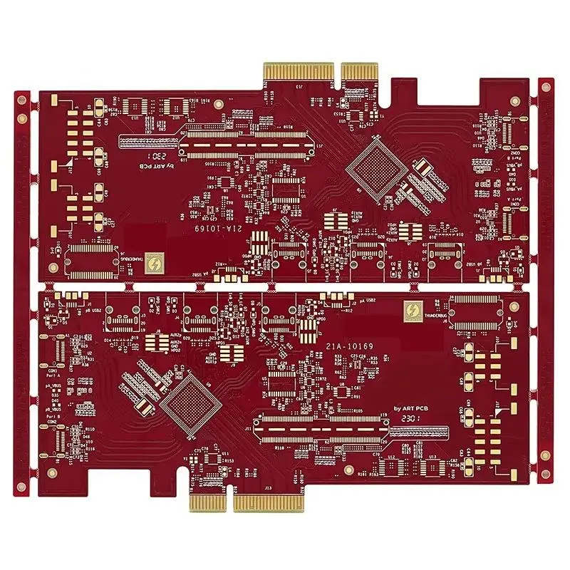
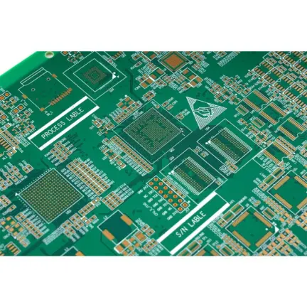
Ball Grid Array (BGA) packages are central to modern electronics, enabling high-density interconnections for advanced components like FPGAs, GPUs, and processors. The manufacturing of printed circuit boards (PCBs) for BGA assembly demands strict adherence to specific parameters. Precise control over these specifications is critical for ensuring solder joint reliability, signal integrity, and overall product longevity. This document outlines the fundamental manufacturing specifications for a standard BGA PCB.
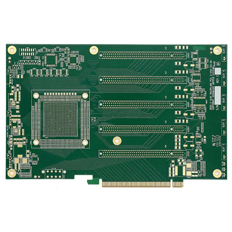
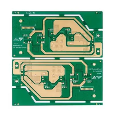
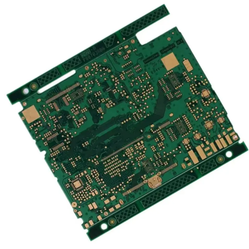
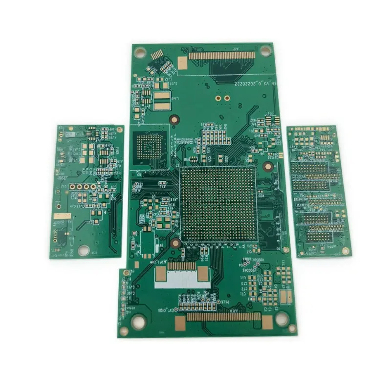
The foundation of a reliable BGA PCB is its substrate. The specified material is FR-4, a flame-retardant epoxy laminate that offers an excellent balance of mechanical strength, electrical insulation, and cost-effectiveness. This particular board is defined as a multilayer construction, which is necessary for routing the complex networks of signals, power, and ground planes required by BGA components. The finished board thickness is controlled to 1.2mm, a common standard that provides rigidity without excessive thickness.
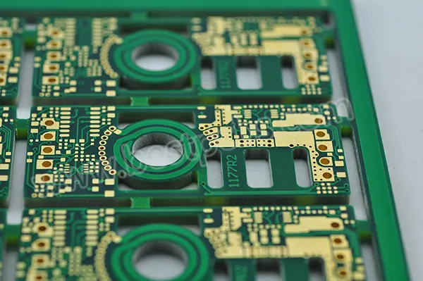
Minimum Trace/Space: This board specifies a minimum trace width and clearance of 4 mils (0.10mm). This level of precision is essential for routing channels between the dense via patterns under the BGA footprint. Consistent control of these dimensions is necessary to prevent issues like shorts (due to insufficient spacing) or opens (due to under-etching).
The chosen surface finish, Immersion Gold (also known as Electroless Nickel Immersion Gold - ENIG), is particularly well-suited for BGA applications. It provides a flat, planar surface, which is crucial for the reliable placement of fine-pitch BGA spheres. The nickel layer acts as a robust diffusion barrier, while the thin gold layer protects the nickel from oxidation during storage, ensuring a highly solderable surface for strong intermetallic bond formation.