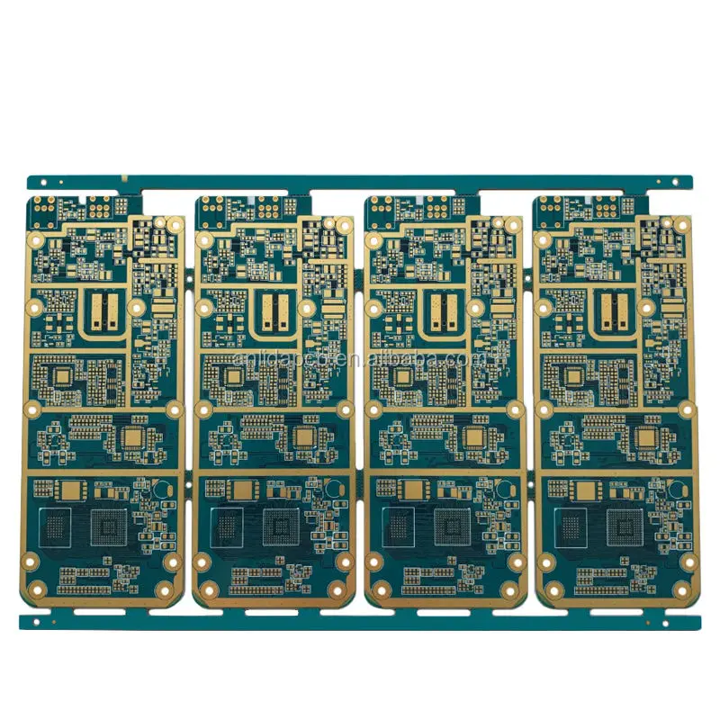
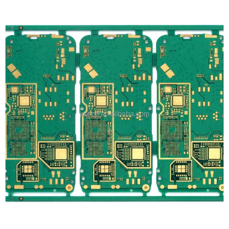
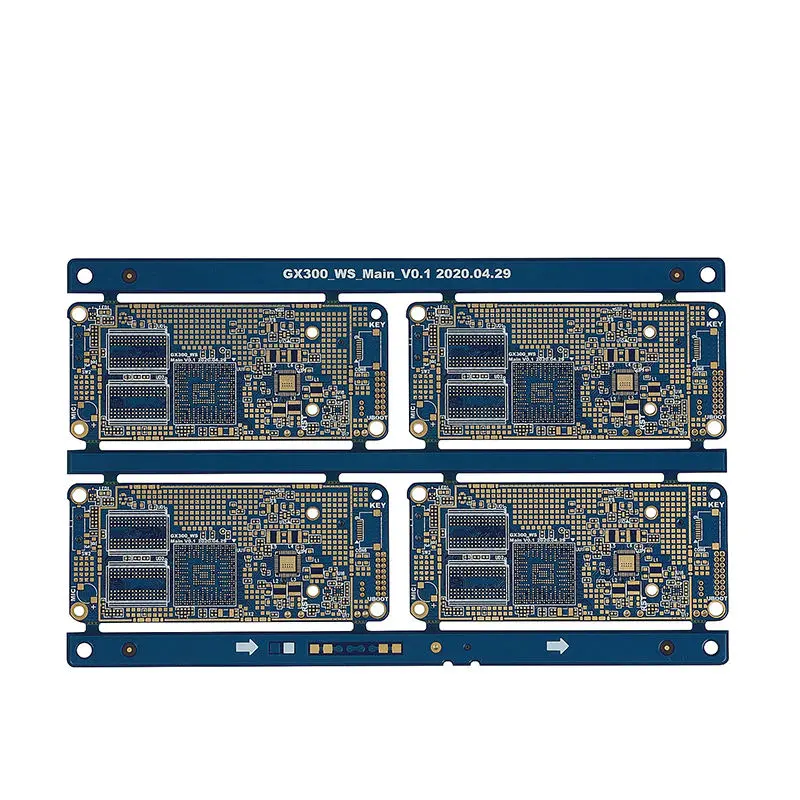
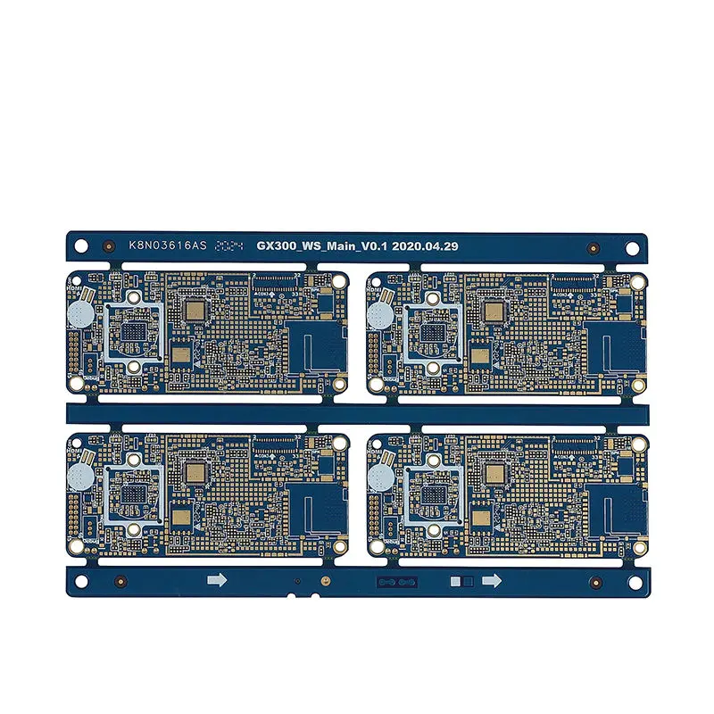
Technical Specifications: High-Performance Halogen-Free PCB for Display Backplanes
This article details the manufacturing specifications for a high-density interconnect (HDI) printed circuit board (PCB) engineered specifically for advanced display backplane applications. This board is designed to meet stringent requirements for performance, reliability, and environmental compliance.
Core Product Overview
1、Product Model: Halogen-Free Display Backplane PCB
2、Base Material: S1150G Halogen-Free Laminate
3、Layer Construction: 10-Layers
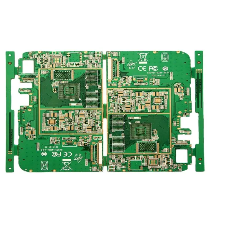
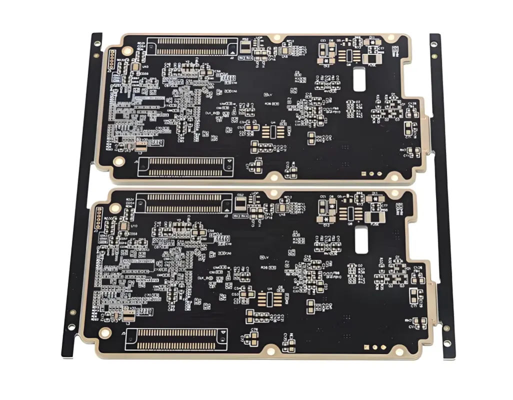
4、Primary Application: This PCB is specifically engineered to serve as the core backplane for modern display modules, ensuring stable signal transmission and structural integrity.4
Detailed Manufacturing Specifications
The following parameters define the board's technical capabilities and manufacturing standards:
1、Board Structure and Material:
Layer Count: 10 layers, supporting complex circuit routing and power distribution.
Base Laminate: S1150G, a halogen-free material that complies with international environmental regulations (HF PCB).
Final Board Thickness: 0.8 millimeters (±10%), providing a slim profile for compact display designs.
2、Circuitry and Signal Integrity:
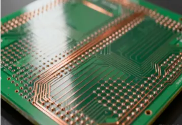
Minimum Trace Width: 3 mils (0.075 millimeters).
Minimum Spacing (Line/Space): 3 mils (0.075 millimeters).
Finished Copper Weight: 0.5 oz, optimized for fine-line circuitry.
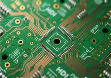
These specifications indicate a high-precision manufacturing process capable of dense circuit layouts essential for high-resolution displays.
3、Surface Finish and Solder Mask:
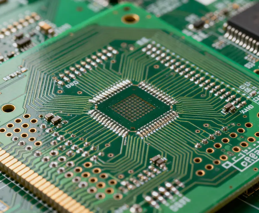
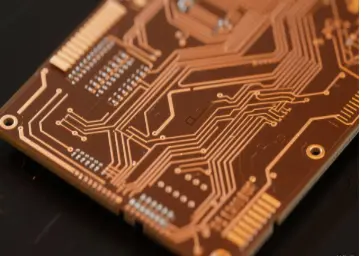
Surface Finish: Electroless Nickel Immersion Gold (ENIG). This finish provides a flat surface, excellent solderability, and long-term shelf life.
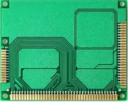
Solder Mask Color Options: Green (standard) or White, often used for LED backlighting applications to enhance reflectivity.
Key Characteristic and Compliance
A defining feature of this PCB is its Halogen-Free compliance. The use of halogen-free materials (S1150G laminate and compatible inks) makes this board a more environmentally sustainable choice, aligning with global initiatives like RoHS and reducing the emission of toxic substances.
This Display Backplane PCB represents a sophisticated solution for the electronics industry, combining high-density design rules with halogen-free materials. Its 10-layer construction, 3mil line/space capability, and robust ENIG surface finish make it a reliable and high-performance choice for demanding display technologies. Manufacturers seeking a compliant, high-precision PCB for next-generation displays will find these specifications meet critical engineering requirements.
Model Number: Display Backplane Halogen-Free PCB
Base Material: S1150G
Layer Count: 10 Layers
Solder Mask Color: Green/White
Final Board Thickness: 0.8mm
Finished Copper Weight: 0.5 oz
Surface Finish: Electroless Nickel Immersion Gold (ENIG)
Minimum Trace Width: 3 mil (0.075 mm)
Minimum Spacing: 3 mil (0.075 mm)
Key Characteristic: Halogen-Free Compliant (HF PCB)
Primary Application: Halogen-Free Display Backplane PCB