Printed Circuit Board")
 Printed Circuit Board")
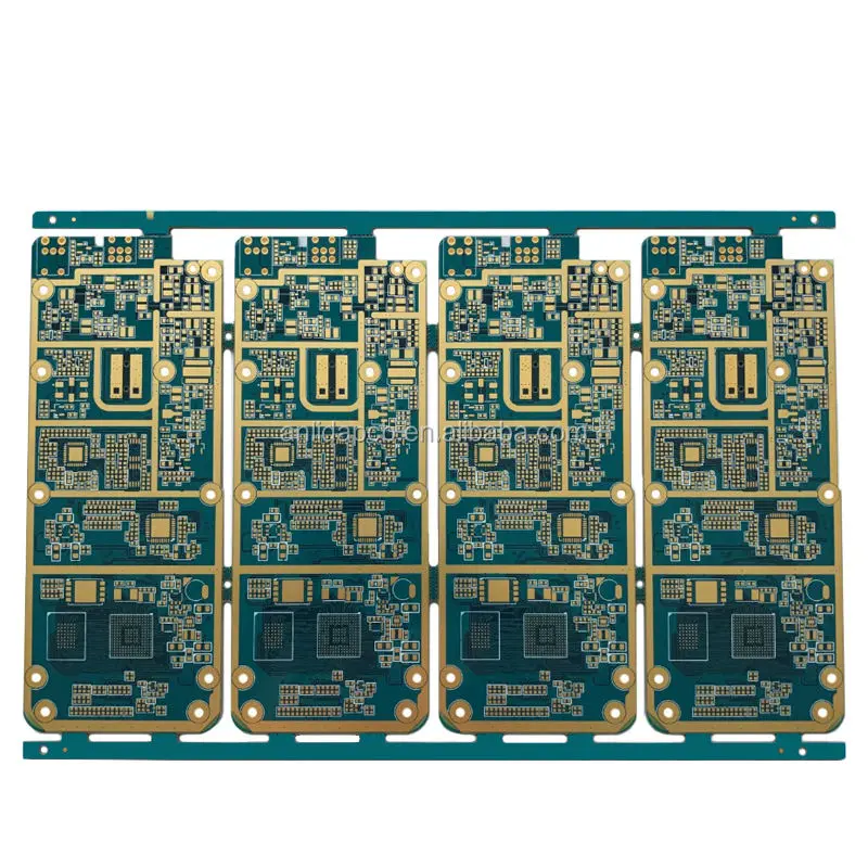
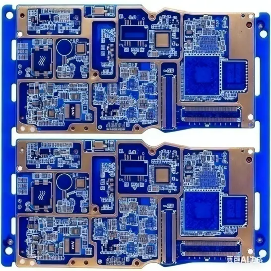
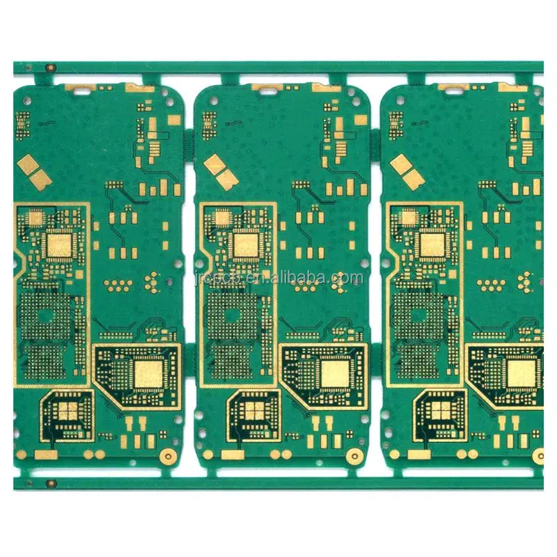
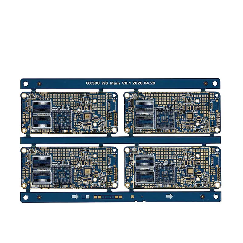
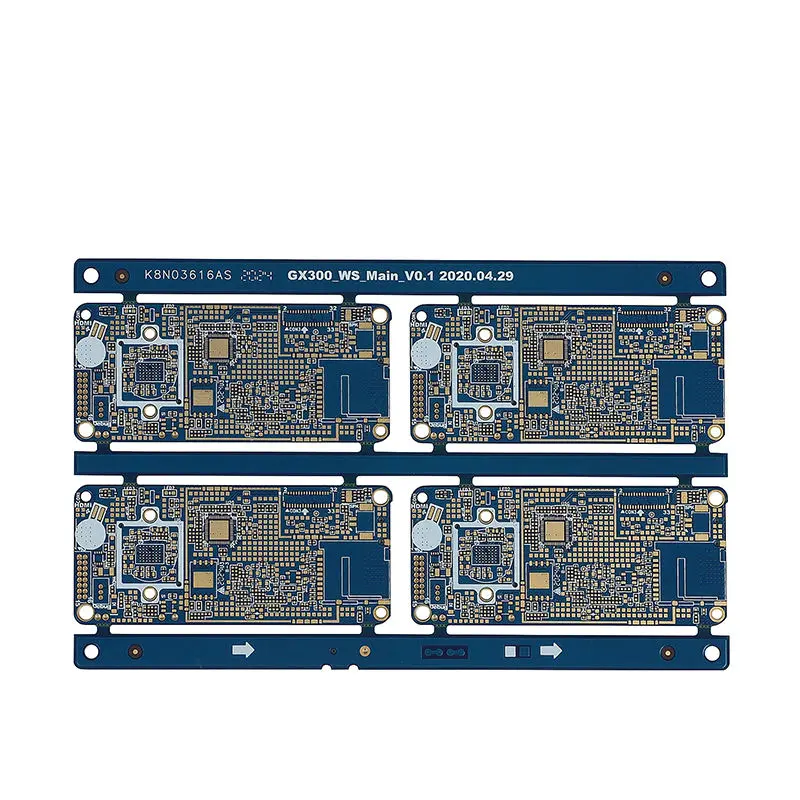
High‑Density Interconnect (HDI) printed circuit boards are the backbone of modern, compact, and high‑speed digital electronics. This technical article provides a detailed analysis of a standard 8‑layer HDI PCB stack‑up, specifically engineered for demanding digital applications. We will break down its key specifications and explain the manufacturing implications of each parameter.
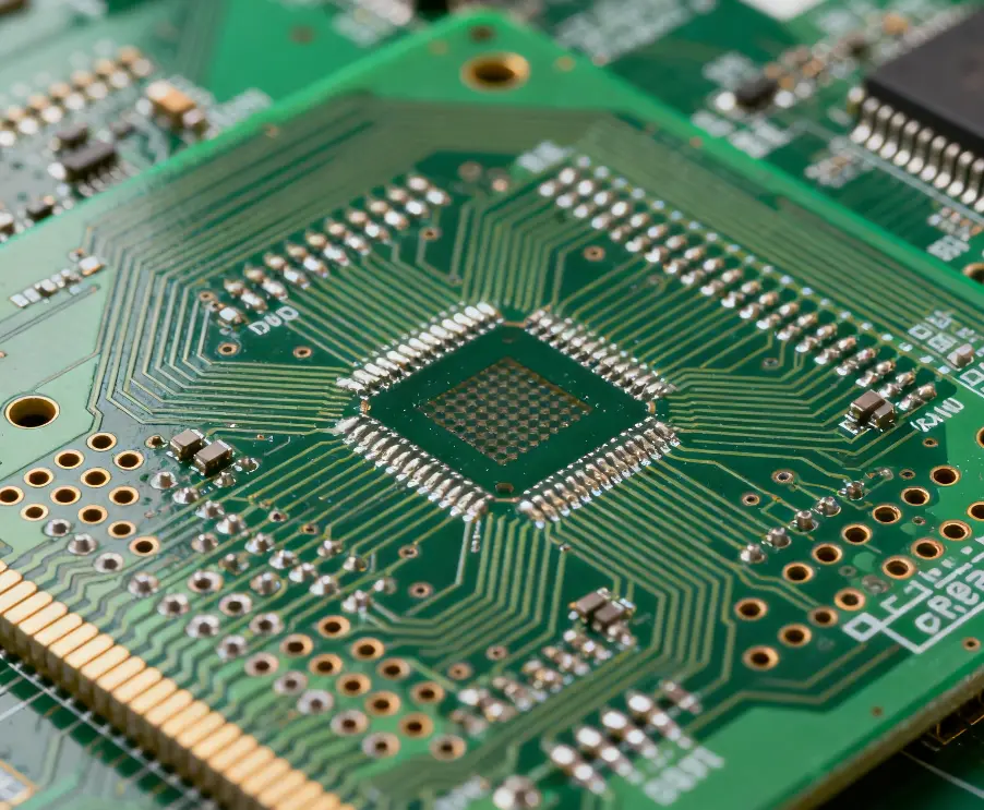
The core of this design is its 2+4+2 HDI buildup construction. This sophisticated architecture signifies a sequential lamination process:
The central 4‑layer core provides robust power and ground planes, ensuring stable voltage delivery and effective EMI shielding.
This core is then laminated with two additional 2‑layer HDI sequences on the outer sides. This structure enables the use of microvias (laser‑drilled holes) for dense component interconnection.
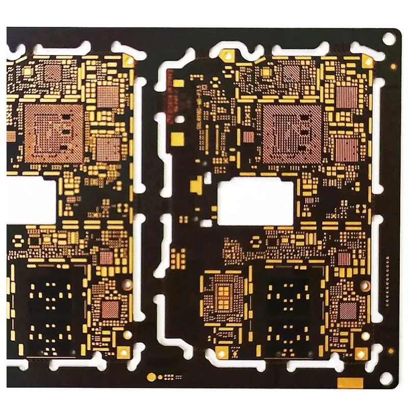
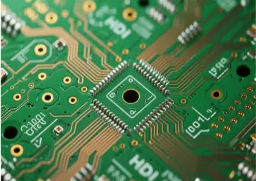
The primary advantage of this build‑up is its ability to facilitate extremely high wiring density, which is critical for components like fine‑pitch BGAs found in modern processors and FPGAs.
The specified base material, IT180A, is a high‑performance laminate known for excellent thermal reliability and electrical properties. Its use is indicative of a design that prioritizes signal integrity and long‑term stability under thermal stress, making it suitable for devices that undergo frequent power cycles or operate in challenging environments.
Finished Board Thickness:
The final thickness is controlled to a precise 1.0 mm. This slim profile is essential for the slim form factors required in contemporary digital products like smartphones, tablets, and ultra‑thin laptops.
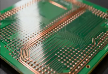
Copper Thickness:
The consistent 0.5 oz (1/1 oz finished) copper weight for both inner and outer layers offers an optimal balance. It allows for the fabrication of fine traces while maintaining sufficient current‑carrying capacity for standard digital signals.
High‑Density Routing Capability:
The specification of a minimum trace/space of 3/3 mil within the BGA area is a hallmark of HDI technology. Achieving this level of precision requires advanced laser direct imaging (LDI) and precise etching control, enabling the routing of connections to today's complex integrated circuits.
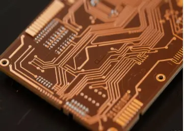
Surface Finish: Immersion Gold (ENIG)
The application of Immersion Gold (ENIG) as the surface finish is an industry‑standard choice for digital HDI PCBs. It provides:
A flat, planar surface, crucial for the reliable soldering of components with a high pin count.
Excellent oxidation resistance, ensuring a long shelf life.
A robust contact surface for gold fingers or test points.
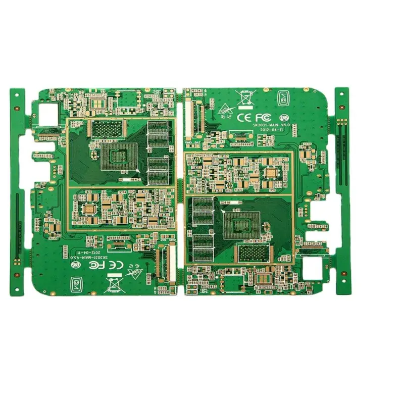
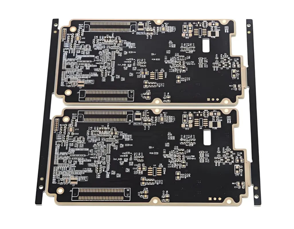
This 8‑layer HDI PCB, with its 2+4+2 construction, IT180A material, and 3/3 mil BGA capability, is ideally suited for the core logic boards of advanced digital products. Typical applications include motherboards for computing platforms, high‑end telecommunications equipment, and sophisticated consumer electronics where performance, reliability, and miniaturization are paramount.
Manufacturing such a board requires a PCB fabricator with proven expertise in HDI processes, including laser drilling, precise layer‑to‑layer registration, and controlled impedance management. Understanding these specifications is the first step in selecting the right manufacturing partner for your next‑generation digital product.