High-Density Interconnect (HDI) printed circuit boards (PCBs) have become essential in modern communication infrastructure, where miniaturization, signal integrity, and thermal reliability are critical. This article details the fabrication of a 12-layer 3rd-order HDI PCB, specifically engineered for high-speed communication applications such as routers, switches, and baseband units.
Stack-Up Architecture and Material Selection
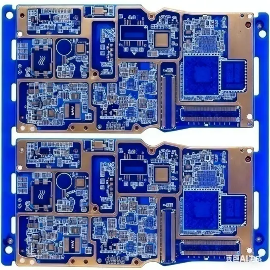
"The PCB employs a 3+6+3 stack-up configuration, which denotes three sequential lamination cycles: two outer HDI layers built upon a 6-layer core. This architecture enables multiple buried and blind vias while maintaining controlled impedance across high-frequency traces.
The base dielectric material selected is TU872slk, a high-performance, halogen-free laminate from TUC (Taiwan Union Technology Corporation). TU872slk offers a low and stable dielectric constant (Dk ≈ 3.78 @ 10 GHz) and dissipation factor (Df ≈ 0.008), making it ideal for high-speed digital and RF applications up to multi-gigabit data rates. Its excellent thermal reliability (Tg > 180°C, Td > 340°C) ensures robust performance under lead-free reflow conditions."
"Electrical and Physical Specifications
1、Finished Board Thickness: 1.2 mm ± 10%
2、Copper Weight: 0.5 oz/ft² (≈17.5 μm) on all layers
3、Minimum Trace/Space: 2.5 mil / 2.5 mil (63.5 μm), achieved through advanced imaging and etching processes
4、Solder Mask: Blue LPI (Liquid Photoimageable) with white silkscreen for optimal contrast and readability
5、Surface Finish: ENIG (Electroless Nickel Immersion Gold)—5–7 μin Ni, 2–4 μin Au—providing flat, oxidation-resistant pads suitable for fine-pitch BGAs and high-reliability solder joints"
HDI Fabrication Process Highlights
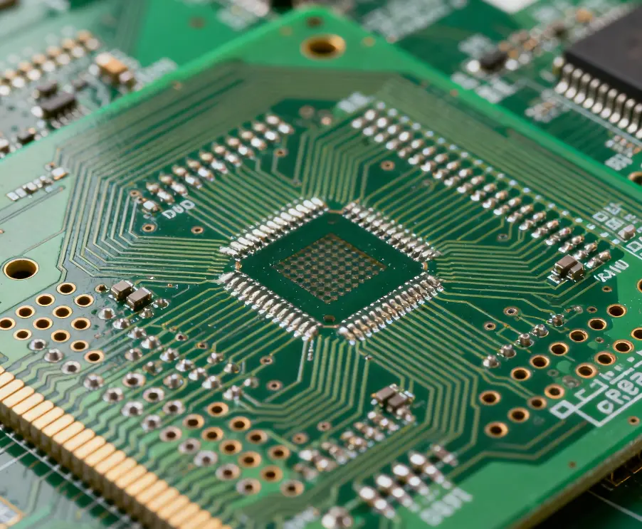
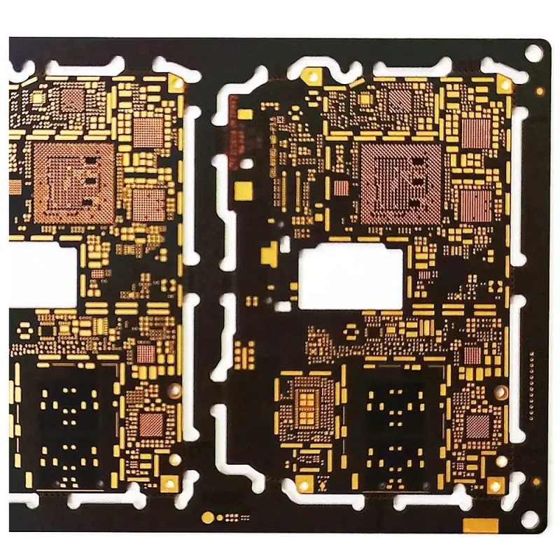
"As a 3rd-order HDI, this design incorporates three levels of microvia stacking or staggering, typically involving:
1、First buildup: Laser-drilled microvias from L1→L2 and L12→L11
2、Second buildup: Additional microvias from L2→L3 and L11→L10
3、Third buildup: Final microvias connecting to the 6-layer core (e.g., L3→L4 and L10→L9)"
All microvias are filled with non-conductive epoxy and planarized to support subsequent copper plating and lamination cycles. Precision laser drilling (typically CO₂ or UV lasers) ensures via diameters as small as 60–80 μm with tight positional accuracy (<25 μm).
Impedance control is rigorously maintained through simulation-driven stack-up design and in-process testing (e.g., time-domain reflectometry). Critical differential pairs for high-speed interfaces (e.g., PCIe, Ethernet) are routed with consistent spacing and reference planes to minimize crosstalk and insertion loss.
Application Context
This PCB is tailored for high-speed communication hardware, where data integrity at multi-gigabit rates is non-negotiable. The combination of fine-line technology, low-loss dielectric, and advanced HDI structure supports dense component placement—such as 0.4 mm pitch BGAs—while preserving signal fidelity and thermal management.
The successful manufacture of a 12-layer 3rd-order HDI PCB using TU872slk demonstrates the convergence of material science, precision fabrication, and signal integrity engineering. As data rates continue to climb in 5G, AI networking, and edge computing systems, such HDI solutions will remain pivotal in enabling next-generation electronic architectures.
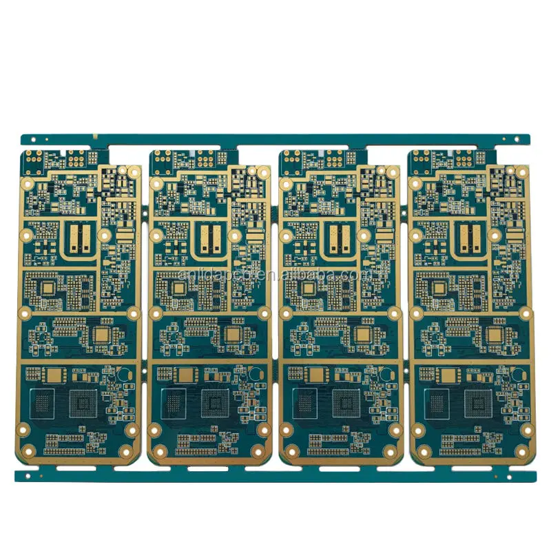
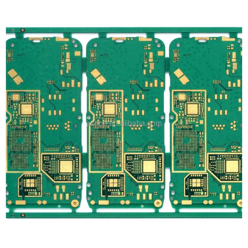
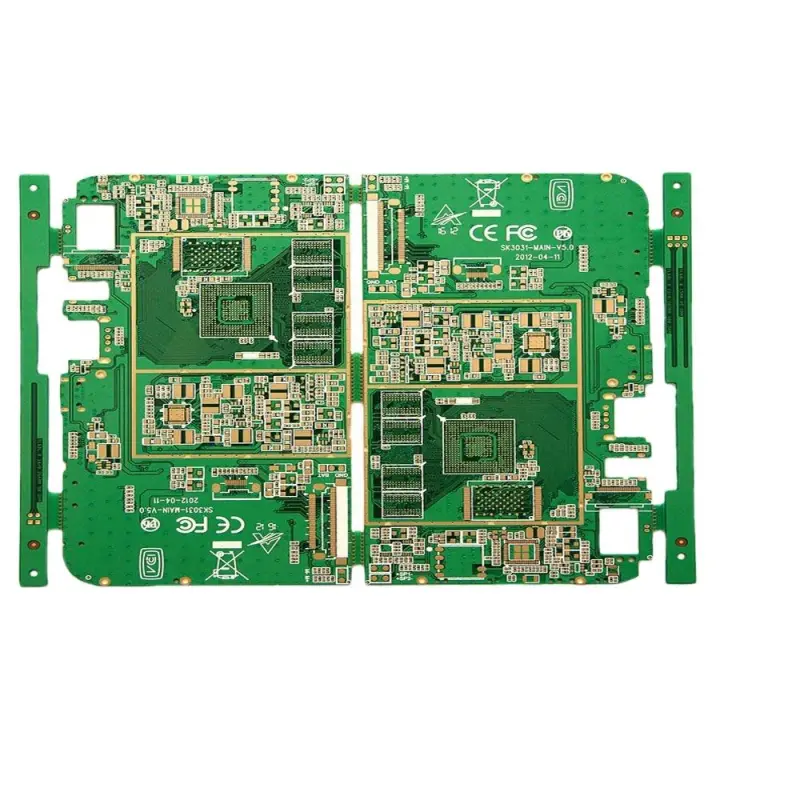
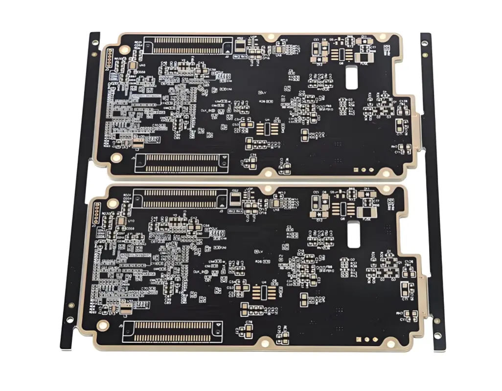
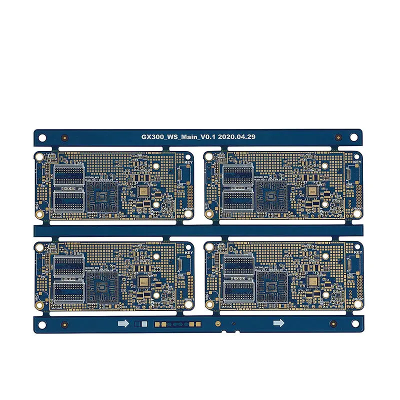
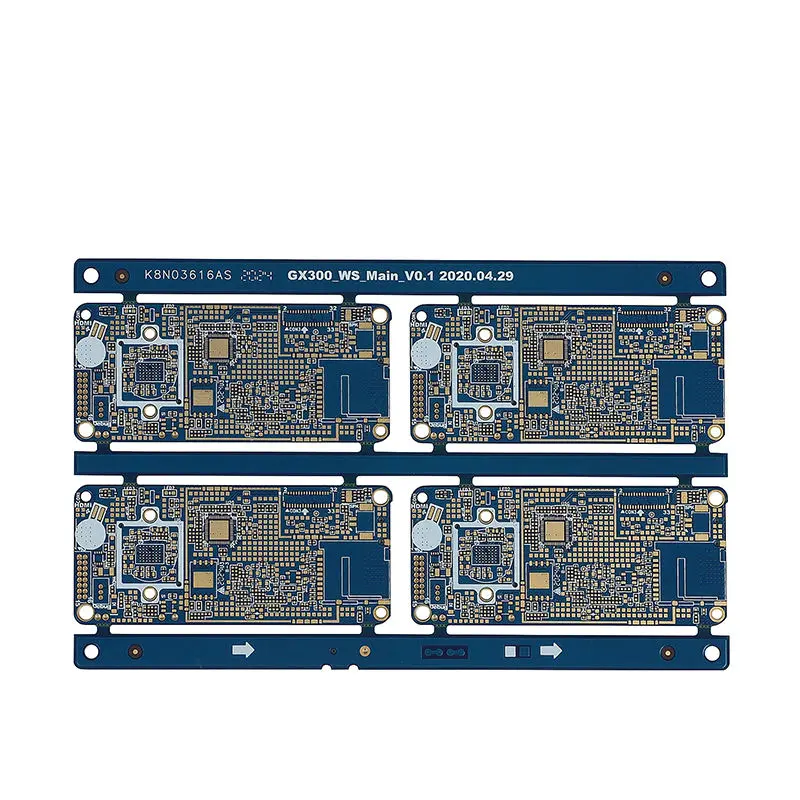
Model: 12-Layer 3rd-Order HDI Communication PCB
Layer Count: 12 Layers
Base Material: TU872slk (High-Performance FR-4 Equivalent)
Finished Thickness: 1.2 mm
Copper Weight: 0.5 oz/ft² (Approx. 17.5 μm)
Color: Blue Solder Mask / White Silkscreen
Surface Finish: Immersion Gold (ENIG – Electroless Nickel Immersion Gold)
Special Technologies: None (Standard HDI Process)
Minimum Trace & Space: 2.5 mil / 2.5 mil (63.5 μm / 63.5 μm)
Application: High-Speed Communication Equipment PCBs (e.g., Routers, Switches, Telecommunication Modules)