")
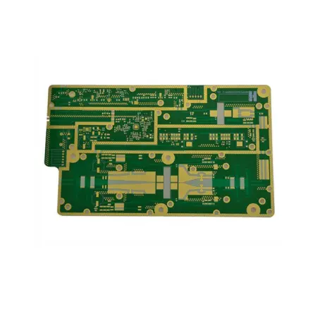
Hybrid Printed Circuit Boards (PCBs) represent a specialized segment of circuit board manufacturing, engineered to meet the demanding requirements of advanced electronics. By combining materials with disparate electrical properties, such as Teflon (PTFE) , ceramic, and standard FR‑4, hybrid constructions offer an optimized solution for applications where signal integrity and thermal management are paramount. This article provides a detailed technical examination of hybrid PCB specifications, materials, and their primary application in high‑frequency microwave circuitry.
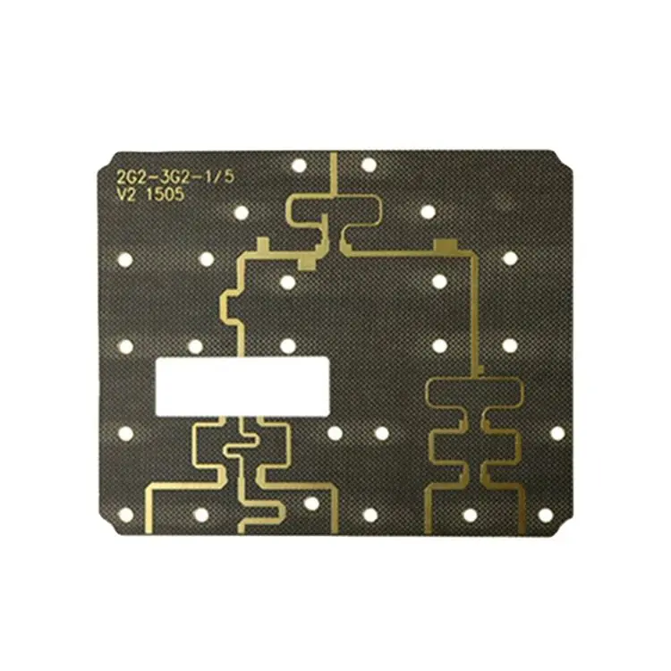
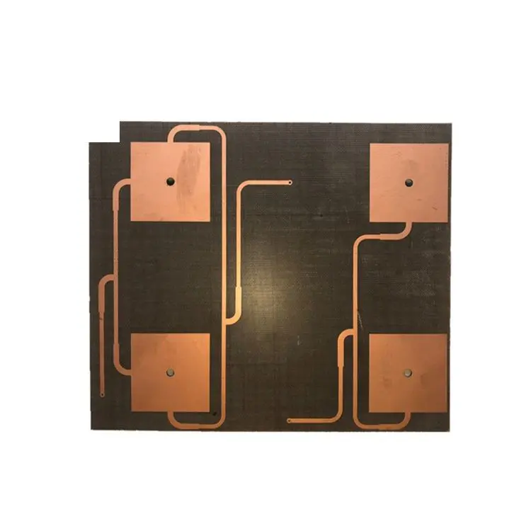
The defining characteristic of a hybrid PCB is its use of a composite substrate. Typically, this involves laminating a high‑frequency material like Teflon or a ceramic‑filled substrate with a standard FR‑4 epoxy laminate. This approach achieves a balance between performance and cost‑effectiveness.
A critical parameter in these applications is the dielectric constant (Dk) . The hybrid material system allows for a wide effective Dk range of 2.2 to 16.0, providing design engineers with significant flexibility:
Low Dk (closer to 2.2): Ideal for high‑speed signals, minimizing propagation delay and signal loss.
Higher Dk: Facilitates circuit miniaturization.
To ensure reliability, hybrid PCBs are manufactured in compliance with IPC‑6012 Class 2/3 qualifications. This certification dictates the stringent acceptance criteria for complex multilayer boards, guaranteeing robustness for commercial (Class 2) and high‑reliability aerospace or military applications (Class 3).
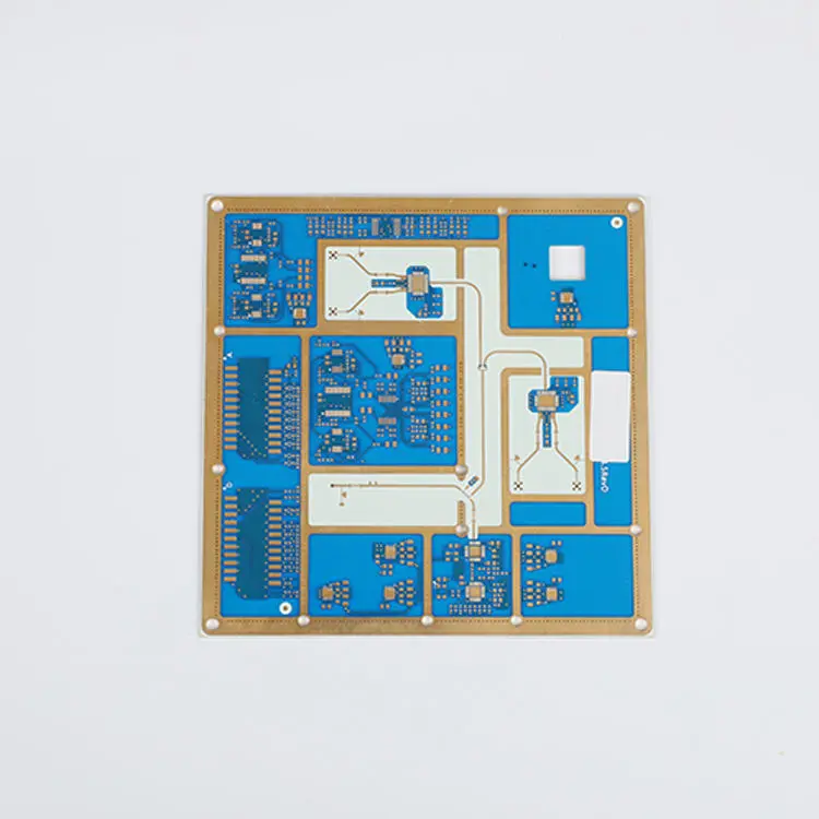
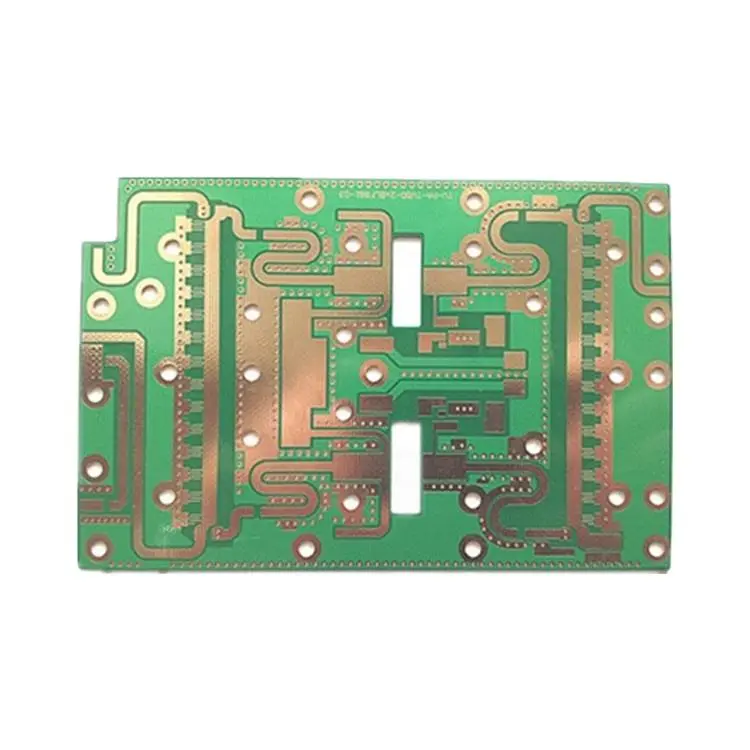
The versatility of hybrid PCB technology supports a broad spectrum of design configurations:
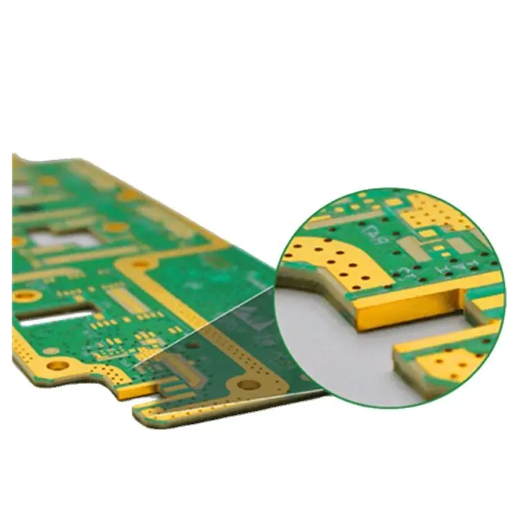
Layer Count: Architectures range from simple 2‑layer boards to complex multilayer constructions, often exceeding 20 layers for sophisticated RF systems.
Board Thickness: Final thickness can be precisely controlled from a thin 0.1 mm to a robust 12.0 mm, accommodating various mechanical and electrical constraints.
Copper Thickness: Copper weights are available from 0.5 oz to 3.0 oz per square foot, allowing designers to tailor current‑carrying capacity and impedance profiles.
Surface Finishes: Multiple surface finish options are offered to suit the assembly process and end‑use environment. Common choices include:
Immersion Silver: Provides a flat surface for fine‑pitch components and offers excellent solderability.
Electrolytic Hard Gold: Delivers superior wear resistance for edge connectors and test points.
Organic Solderability Preservative (OSP): A cost‑effective, RoHS‑compliant finish for standard assembly processes.
The principal application domain for hybrid PCBs is in high‑frequency microwave electronics. This includes:
Radar and Satellite Communication Systems
5G Telecommunications Infrastructure
Aerospace and Defense Electronics
Advanced Medical Imaging Equipment
The ability to integrate low‑loss Teflon circuits for RF signal paths with robust FR‑4 sections for power and control logic makes hybrid technology indispensable in these fields.
Hybrid PCBs are a critical enabling technology for modern high‑performance electronics. Their unique material composition, governed by precise specifications for dielectric constant, layer construction, and quality standards, makes them the substrate of choice for challenging high‑frequency applications. Understanding these technical parameters is essential for design engineers, procurement specialists, and anyone involved in developing next‑generation electronic systems.