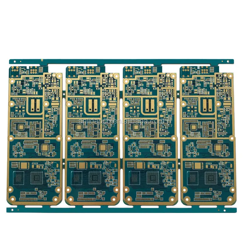
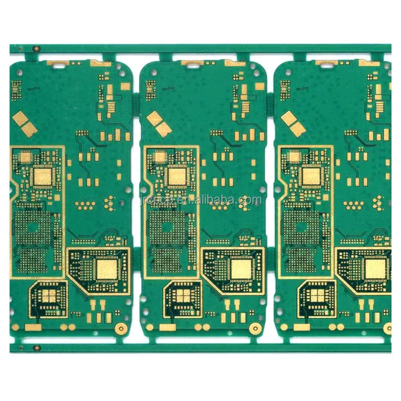
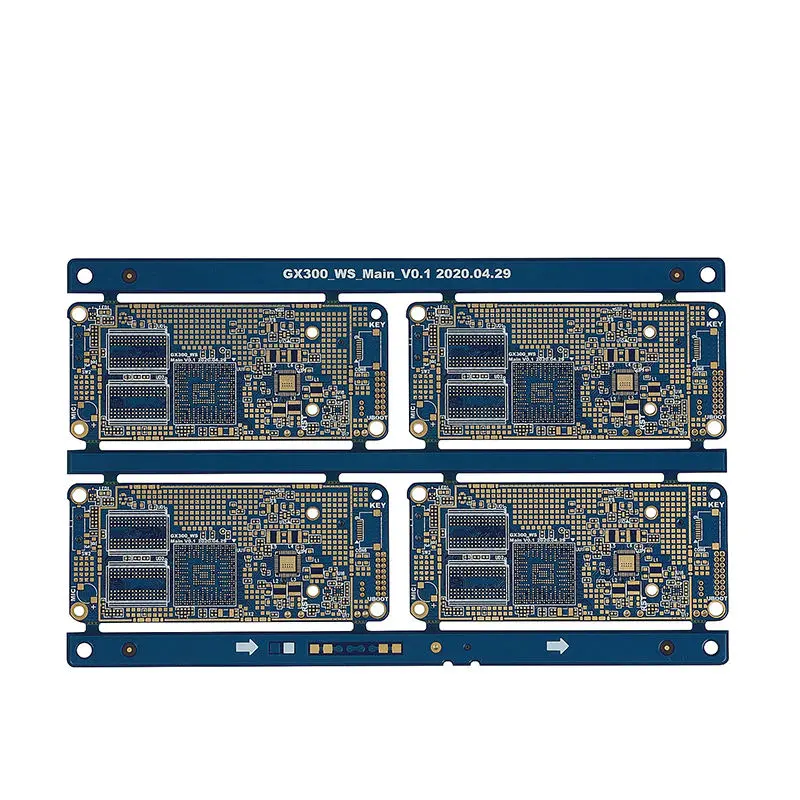
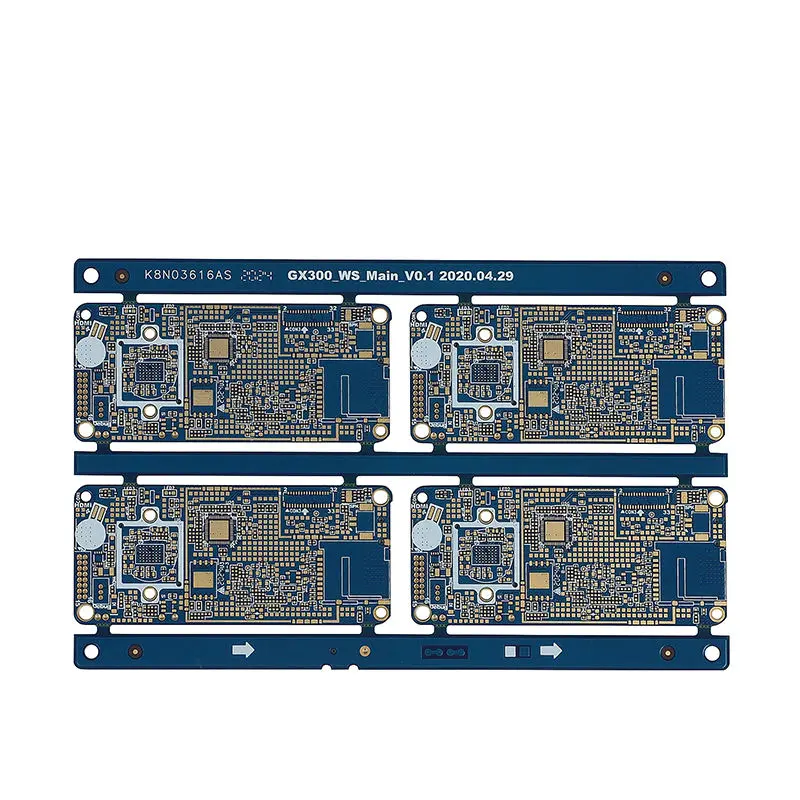
Engineering a High-Density Micro SD Card PCB: A Technical Overview
The relentless drive for higher data storage capacity in smaller form factors places immense demands on the underlying printed circuit board. The Micro SD card PCB is a critical component where precision engineering meets advanced materials science. This article details the key specifications and manufacturing considerations for a high-performance, 6-layer HDI PCB designed specifically for next-generation Micro SD applications.
Core Material: Isola FR408 High-Performance Laminate
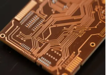
At the heart of this PCB is the Isola FR408 high-Tg laminate. This material is selected for its superior electrical properties, including a stable and low dielectric constant (Dk), which is crucial for maintaining signal integrity at high speeds. FR408 offers excellent thermal performance, with a high glass transition temperature (Tg) that ensures dimensional stability during soldering processes and under operational stress. Its robustness makes it an ideal choice for reliable, high-yield manufacturing.
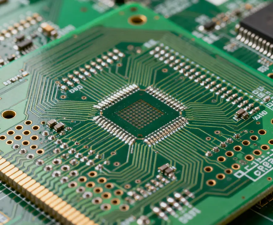
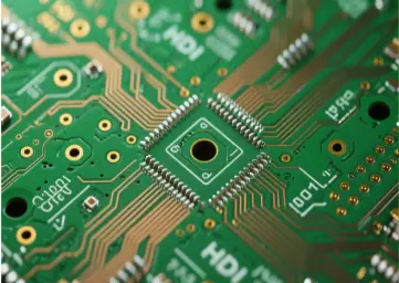
Advanced Board Construction: 6-Layer 2+N+2 HDI Stack-up
The board features a sophisticated 6-layer construction utilizing a 2+N+2 any-layer HDI (High-Density Interconnect) methodology. This architecture is essential for achieving the high wiring density required by complex memory controllers in a minimal footprint.
"2+N+2" Breakdown: The design starts with a core (N), which is then built up sequentially with two additional layers on both the top and bottom. This approach allows for the use of laser-drilled microvias, which are significantly smaller than mechanically drilled through-holes. Microvias enable more direct routing paths, reducing signal propagation delay and freeing up valuable real estate for component placement.
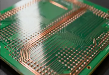
Precision Thickness and Copper Weights
"Achieving an ultra-thin profile is non-negotiable for compliant Micro SD card design.
1、Finished Board Thickness: The final thickness is controlled to a precise 0.3mm. This requires meticulous control during the lamination and planarization processes to ensure uniformity across the entire panel.
2、Copper Thickness Specification: The specification of 1/3 oz (approximately 12µm) for inner layers and 0.5 oz (referred to as ""0 oz"" in the spec, typically meaning ½ oz or ~17.5µm base foil) for outer layers is a critical design choice. Thinner inner-layer copper minimizes the potential for resin starvation, while the standard outer-layer copper is optimized for fine-line circuitry and reliable solder joint formation."
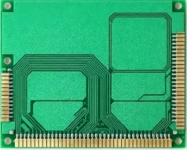
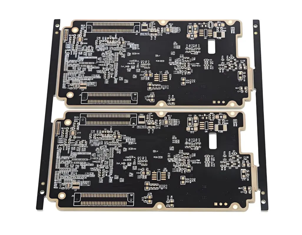
Solder Mask and Aesthetic Options
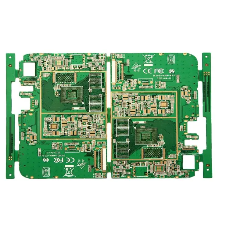
To meet various product branding requirements, this Micro SD card PCB is available with high-resolution solder mask in either black or white. The solder mask is applied with precision to ensure perfect definition of exposed pads and to provide durable environmental protection for the delicate circuitry.
"This specific combination of a high-performance laminate like Isola FR408, an advanced 2+N+2 HDI stack-up, and ultra-precise thickness control results in a Micro SD card PCB that meets the rigorous demands of modern data storage. It delivers the necessary signal integrity, thermal resilience, and physical robustness required for high-capacity, high-speed memory applications, making it a premier choice for electronics manufacturers pushing the boundaries of miniaturization.
For inquiries regarding this Micro SD card PCB or to discuss customizing the specifications for your application, please contact our engineering team."
Substrate Material: Isola FR408 (High-Performance Flame-Retardant Laminated Material)
Layer Configuration: 6-Layer, 2+N+2 HDI (High-Density Interconnect) Structure
Surface Finish Color: Black / White
Final Board Thickness: 0.3 mm