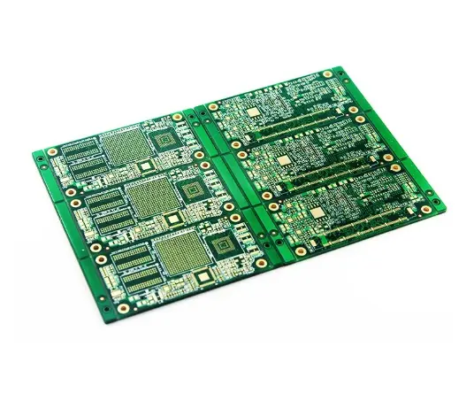
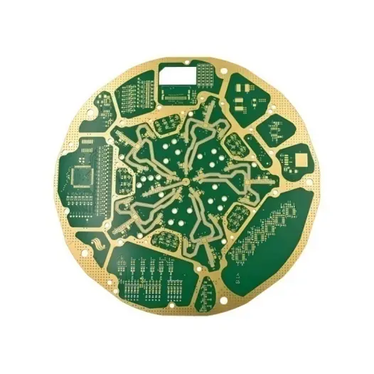
Technical Specifications: 20-Layer High-Speed PCB for Communication Backplane Systems
This technical datasheet outlines the specifications of a 20-layer high-speed Printed Circuit Board (PCB) engineered for high-performance communication backplane applications. The board is designed to meet stringent requirements for signal integrity, structural reliability, and dense interconnects in advanced telecommunications infrastructure.
"Key Manufacturing Specifications and Construction Details
1、Model & Function: 20-Layer High-Speed PCB
2、Construction Material: The laminate system utilizes TUC / TU872LK, a high-performance material chosen for its excellent dielectric properties, thermal stability, and low signal loss at high frequencies, which is critical for backplane operations.
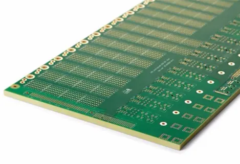
3、Layer Configuration: 20 Layers
4、Finished Board Thickness: 5.0 mm (±10%). This controlled thickness ensures mechanical stability and compatibility with standard backplane connectors and enclosures.
5、Copper Thickness: Consistent 1-ounce (1OZ) copper weight on both inner and outer layers. This standardization supports controlled impedance for high-speed signals and efficient power distribution.
6、Solder Mask & Legend: Available in Green or White solder mask, providing environmental protection and clear component designation.
7、Minimum Trace/Space: 4 mil (0.10 mm) / 4 mil (0.10 mm). This fine-line capability allows for high-density circuit routing, essential for complex backplane architectures.
8、Surface Finish (Plating): Hard Gold (Electrolytic Nickel-Gold) with a thickness range of 3 to 15 microns. This robust finish offers superior wear resistance for edge connectors, excellent corrosion resistance, and reliable solderability.
9、Blind Via Architecture: Blind vias are implemented from layer 3 to layer 20 (L3-L20). This sophisticated via-in-pad technology is utilized to optimize signal paths, save space, and enhance routing density in the board's core section.
10、Primary Application: This PCB is specifically designed for use as a Communication Backplane PCB, serving as the fundamental interconnect platform for high-speed data transmission between multiple daughter cards in networking switches, routers, and server systems."
Engineering and Manufacturing Value
This 20-layer PCB specification reflects a design focused on high-speed performance and reliability. The combination of TU-series laminates, precise impedance control through uniform copper weight, fine-line etching, and a durable hard gold finish makes it suitable for demanding operating environments. The defined blind via structure addresses the need for complex interconnect solutions without compromising the board's structural integrity.
Manufactured under strict quality controls, this backplane PCB ensures consistent performance for next-generation communication hardware, supporting high data rates and signal integrity across all layers.
Model: 20-Layer High-Speed PCB
Construction Material: TUC / TU872LK
Layer Count: 20 Layers
Final Thickness: 5.0 mm
Copper Thickness (Inner/Outer): 1 OZ
Solder Mask Color Options: Green / White
Minimum Trace/Spacing: 4 mil / 4 mil
Surface Finish: Hard Gold (3–15 μm)
Blind Via Configuration: L3 to L20
Primary Application: Communication Backplane PCB