Engineering a Robust High-Speed PCB for Advanced FPGA Applications
The effective implementation of high-speed FPGAs is critically dependent on the performance and integrity of the underlying printed circuit board (PCB). A board designed for these applications must address signal integrity, power integrity, and thermal management with precision. The following technical specifications outline the build parameters for a high-reliability PCB engineered to support demanding FPGA-based systems.
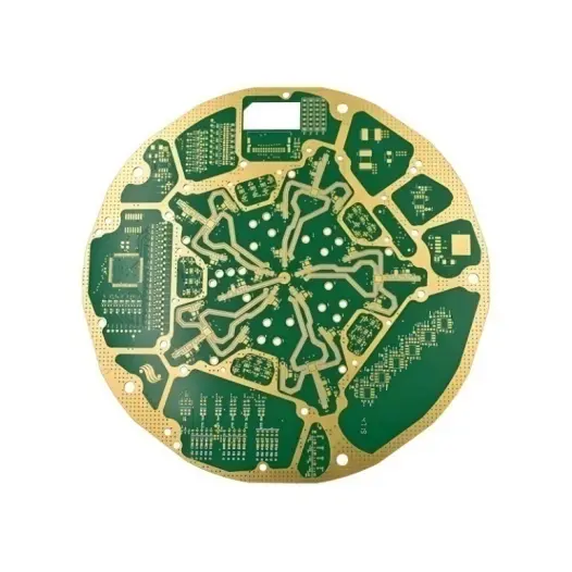
"Critical PCB Construction Specifications
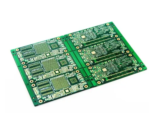
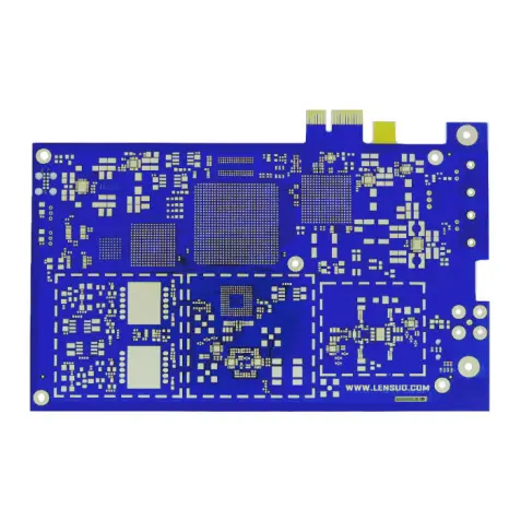
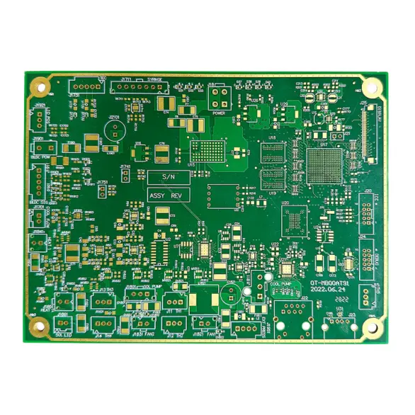
1、Primary Application: This board is specifically designed as a high-speed, high-performance platform for Field-Programmable Gate Array (FPGA) circuits, suitable for use in data acquisition, telecommunications, and advanced processing systems.
2、Base Material: The substrate is a TG180 laminate, a critical choice for stability in high-temperature environments. This material ensures the board's dimensional and electrical stability during assembly reflow cycles and throughout its operational life, which is essential for complex, dense designs.
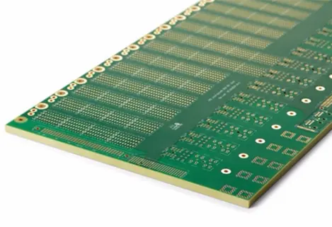
3、Board Stack-Up: The design utilizes a 10-layer stack-up. This multi-layer configuration provides dedicated internal layers for power and ground planes, which are vital for clean power delivery and effective EMI/RFI shielding. The controlled impedance stack-up is fundamental for managing high-speed signal paths and minimizing crosstalk.
4、Finished Board Thickness: The final product has a standardized thickness of 1.6mm. This thickness offers a robust mechanical structure that is compatible with standard connectors and enclosure designs, while providing sufficient dielectric space for impedance control.
5、Copper Cladding: Both the inner and outer layers feature a 1-ounce (1 oz) copper weight. This uniform thickness balances current-carrying capacity for power planes with the fine-line etching capabilities required for high-density interconnects on signal layers.
6、Fabrication Tolerances: The board features a minimum trace and space width of 4 mils (4/4 mil). This fine-line geometry is a standard for high-density interconnect (HDI) PCBs, allowing for the routing of complex FPGA ball grid array (BGA) packages.
7、Surface Finish: The exposed copper pads are treated with a 5-microinch (""U"") hard gold (Electroless Nickel Immersion Gold - ENIG) finish. This surface provides a flat, solderable surface excellent for fine-pitch components, offers superior oxidation resistance for long shelf life, and ensures reliable contact for gold-plated connectors.
8、Solder Mask: The board is finished with a blue/white solder mask, which aids in automated optical inspection (AOI) during the assembly process."
This combination of high-grade materials, precise 10-layer construction, and stringent fabrication tolerances results in a PCB that meets the rigorous electrical and physical demands of modern FPGA applications. By specifying TG180 material, a robust stack-up, and a durable hard gold finish, this design ensures signal integrity, power stability, and long-term reliability for high-speed digital systems. Engineers can leverage these specifications as a benchmark for developing cutting-edge electronic products.
Model: High-Performance FPGA Circuit Board
Construction Material: TG180 Laminate
Layer Count: 10-Layer Stack-up
Board Thickness: 1.6 millimeters
Copper Weight: 1 oz (Inner & Outer Layers)
Solder Mask: Blue/White
Minimum Trace/Spacing: 4/4 mil
Surface Finish: 5μ" Hard Gold
Primary Application: FPGA-Based High-Speed Printed Circuit Board.