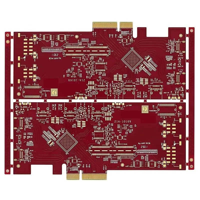
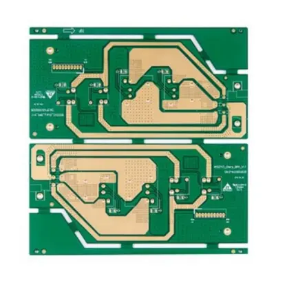
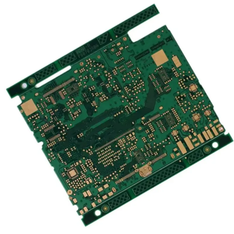
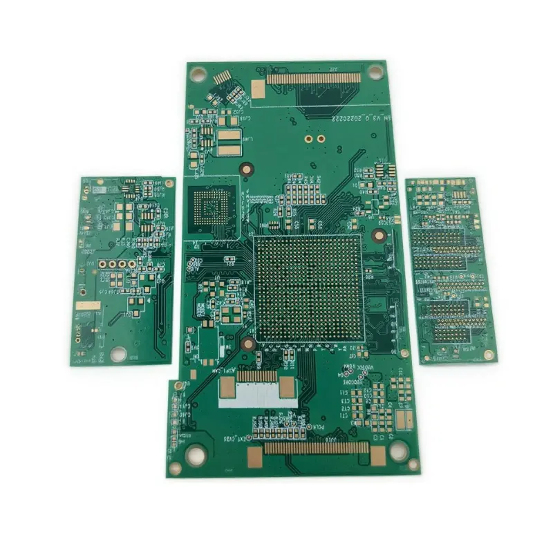
High‑density communication systems demand robust and reliable interconnect solutions at their core. The 24‑layer communication backplane PCB is engineered to meet these stringent requirements, serving as the fundamental backbone for high‑speed data transmission in advanced networking, telecommunications, and data center hardware. This article provides a detailed technical breakdown of its key manufacturing specifications and functional characteristics.
The foundation of this backplane’s performance is its premium base material. Fabricated using Panasonic M6 low‑loss laminate, this PCB ensures excellent signal integrity at high frequencies. The M6 material is selected for its stable dielectric constant, low dissipation factor, and superior thermal reliability, which are critical for minimizing signal attenuation and skew in multi‑gigabit applications.
The 24‑layer (24L) construction is a defining feature, enabling the complex routing necessary for modern high‑pin‑count connectors and processors. This high layer count allows for dedicated power and ground planes, which enhance power distribution and provide critical shielding to reduce electromagnetic interference (EMI) between sensitive signal layers.
Precision manufacturing is evident in the following key parameters:
Finished Board Thickness:
The board is manufactured to a precise thickness of 2.0 mm. This controlled thickness provides the necessary rigidity and structural integrity for a large‑format backplane, ensuring compatibility with standard connectors and chassis designs.
Copper Thickness:
A finished copper weight of 1 oz (OZ) is standard for both internal and external layers. This specification offers an optimal balance between current‑carrying capacity and the ability to etch fine‑line features.
Surface Finish:
The board employs Immersion Gold (ENIG) surface treatment. ENIG provides a flat, solderable surface with a long shelf life, which is essential for the reliable soldering of press‑fit connectors and other components. The gold layer protects the underlying nickel from oxidation, ensuring consistent connectivity.
Minimum Trace/Space:
The design rules support a minimum trace width and spacing of 6 mil (0.15 mm) . This capability is indicative of advanced fabrication processes, allowing for high‑density interconnects (HDI) necessary for routing a vast number of high‑speed differential pairs.
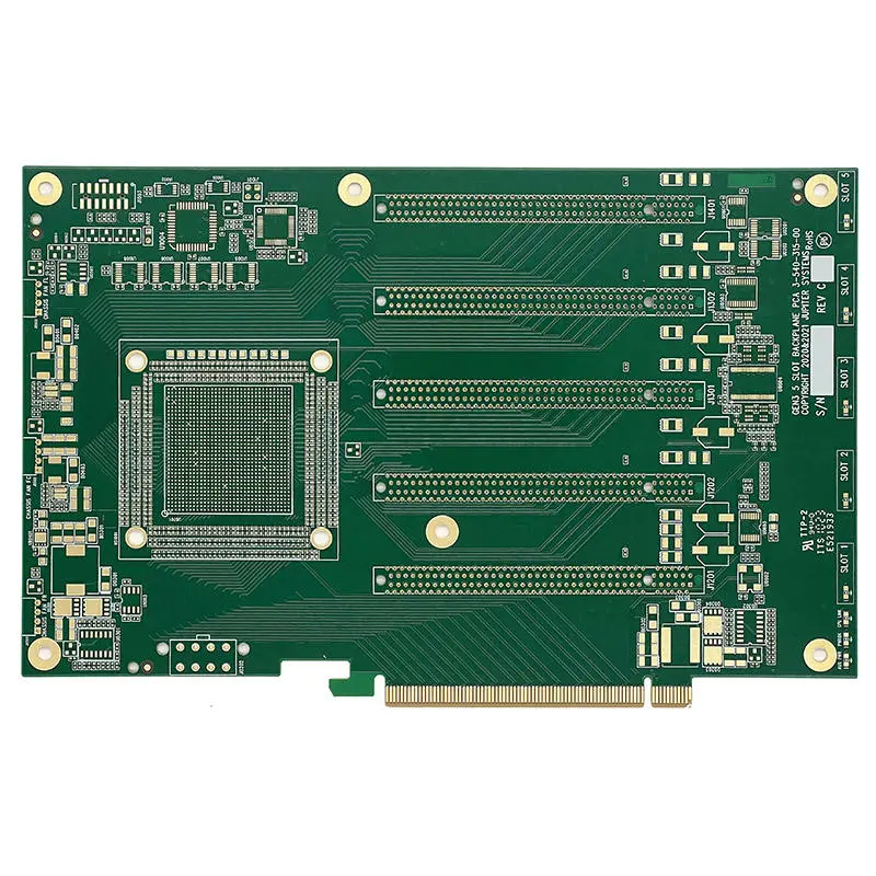
The primary application of this PCB is as a communication backplane. It is designed to function as the central nervous system in equipment such as network switches, routers, servers, and signal processing units. Its high multilayer characteristic is its most significant attribute, enabling it to manage massive data throughput with stability and speed.
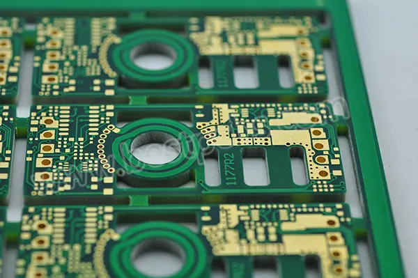
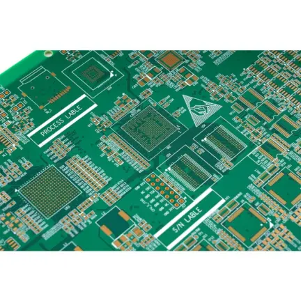
The distinctive blue and white solder mask aids in visual inspection and also serves to protect the delicate circuitry from environmental contaminants and physical damage during handling and assembly.
This 24‑layer backplane PCB, with its Panasonic M6 core, precise 2.0 mm thickness, ENIG finish, and 6 mil trace/space capability, represents a high‑end solution for critical communication infrastructure. Its design and manufacturing specifications are meticulously chosen to ensure maximum signal integrity, power distribution, and long‑term reliability in the most demanding operational environments. Engineers and procurement specialists can specify this board with confidence for next‑generation high‑speed digital systems.