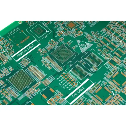
The evolution of automotive electronics—from advanced driver‑assistance systems (ADAS) to complex engine control units (ECUs)—demands printed circuit boards (PCBs) of unparalleled reliability and performance. While the 4‑layer PCB serves as a fundamental building block, high‑performance applications require a more sophisticated foundation: the 14‑layer automotive PCB. This article details the critical manufacturing technologies and specifications that define these high‑density interconnect (HDI) boards, engineered to withstand the harsh environments of modern vehicles.
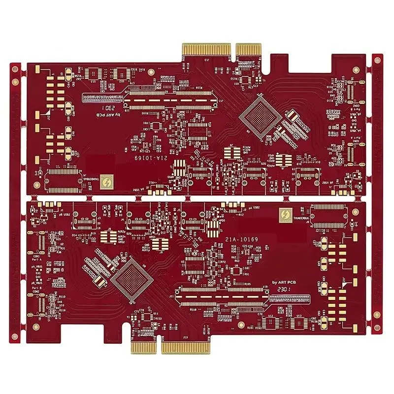
Moving from a standard 4‑layer to a complex 14‑layer build introduces significant engineering considerations. The following specifications represent a typical high‑reliability stackup:
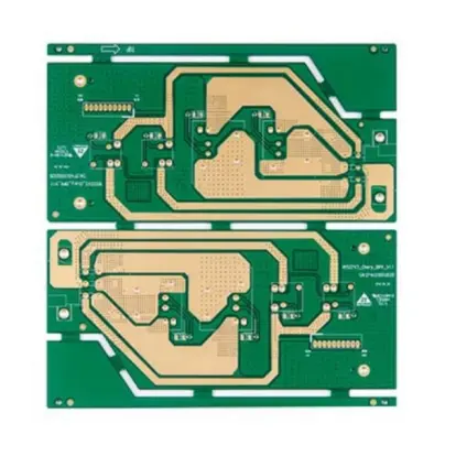
Layer Count: 14‑Layers
Board Thickness: 2.0 mm (Finished, typical)
Base Material: High‑Tg FR‑4 (e.g., Shengyi S1150G or equivalent). High Glass Transition Temperature (Tg) materials (≥150°C) are essential for resisting thermal stress under the hood.
Copper Weight: 1 oz (standard for signal layers), with 2 oz options for dedicated power and ground planes to manage current and heat.
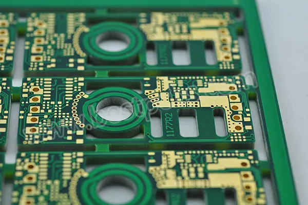
Surface Finish: Immersion Gold (ENIG). This finish provides a flat surface for fine‑pitch components, excellent solderability, and robust wire bonding capability for advanced packaging.
Minimum Trace/Space: 3/3 mil. This tighter tolerance, compared to the standard 4/4 mil, is often necessary to route complex ICs and achieve high signal density.
Controlled Impedance: Critical for signal integrity in high‑speed applications like radar and video processing. Impedance values are tightly controlled during manufacturing as per the design specification.
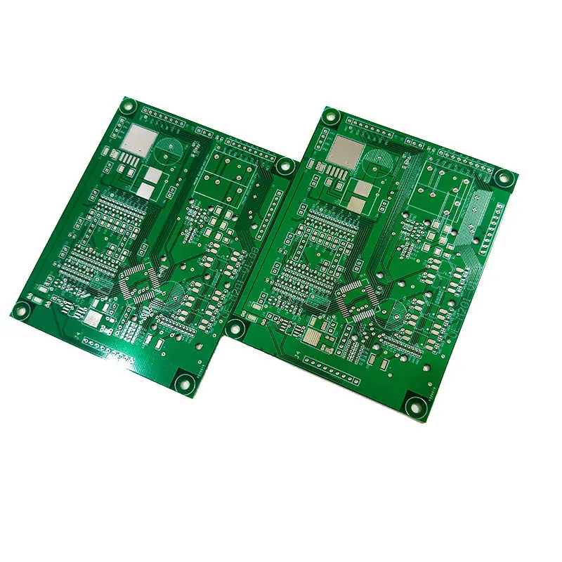
The production of a 14‑layer automotive PCB extends beyond standard multilayer processes. Key technologies include:
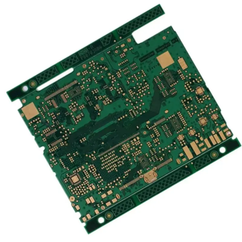
High‑Density Interconnect (HDI): Many 14‑layer boards incorporate HDI technology, utilizing microvias, blind vias, and buried vias. This allows for a higher density of connections in a smaller area, which is crucial for miniaturizing complex ECUs.
Sequential Lamination: The 14 layers are built up in multiple lamination cycles. This process is critical for creating reliable buried vias and managing the increased thickness and internal stress of the board.
Advanced Drilling and Plating: Laser drilling is used for creating small‑diameter microvias. Precise plating processes are essential to ensure uniform copper deposition in the high‑aspect‑ratio through‑holes, guaranteeing electrical connectivity and mechanical strength across all 14 layers.
Automated Optical Inspection (AOI): Every layer is subjected to rigorous AOI to detect defects like shorts or opens. This is a non‑negotiable step for ensuring the functional integrity of a board with such high complexity.
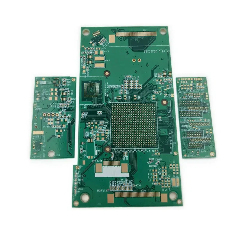
PCBs built to these specifications are designed for the most critical vehicle systems:
ADAS Controllers: For processing data from cameras, LiDAR, and radar, requiring impeccable signal integrity.
Central ECUs: Acting as the vehicle’s central computer, demanding robust power delivery and thermal management.
Powertrain and Battery Management Systems (BMS): For electric and hybrid vehicles, where high current and high‑temperature operation are paramount.
The 14‑layer automotive PCB represents a significant leap in engineering over standard multilayer boards. By leveraging HDI technology, high‑performance materials, and stringent manufacturing controls, these PCBs provide the necessary reliability, density, and signal performance to power the next generation of automotive innovation. When sourcing these critical components, partnering with a manufacturer that specializes in high‑layer‑count and automotive‑grade production is essential for long‑term performance and vehicle safety.