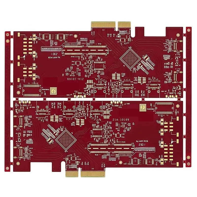
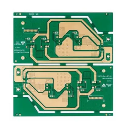
The demand for reliable, high‑speed communication equipment drives the need for printed circuit boards (PCBs) manufactured to exacting standards. This article details the advanced manufacturing technology and specifications for a 10‑layer multilayer PCB engineered specifically for critical communication instrumentation. The design focuses on signal integrity and controlled impedance as its cornerstone.
The foundation of any high‑performance PCB is its substrate material. For this communication instrument PCB, we specify TU‑768 laminate from Taiwan TUC. This high‑frequency laminate is selected for its consistent dielectric constant (Dk) and low dissipation factor (Df), which are critical parameters for maintaining signal integrity at high frequencies. Its thermal stability ensures reliable performance under the operational stresses typical of communication hardware.
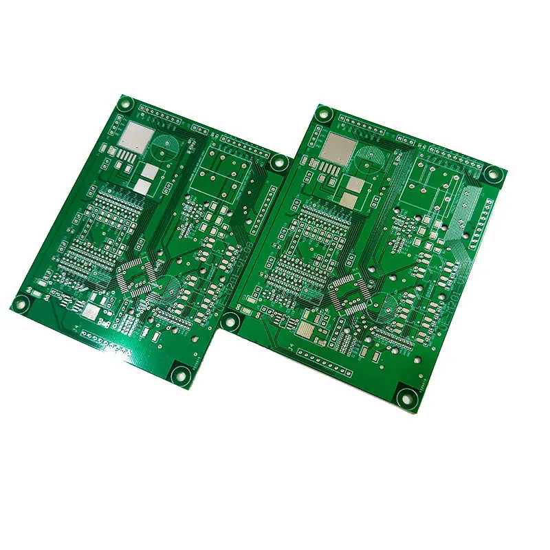
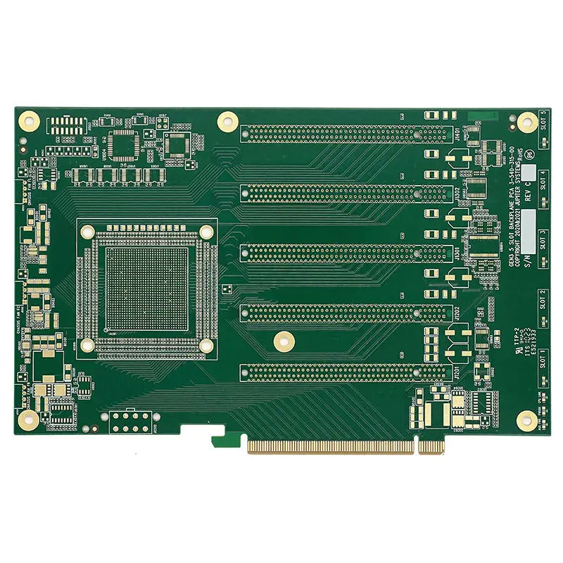
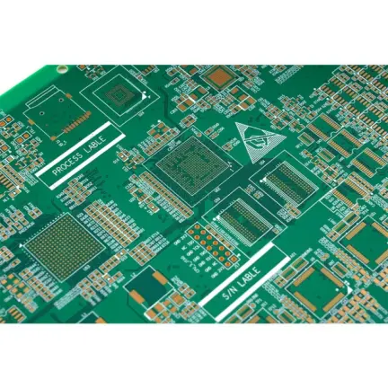
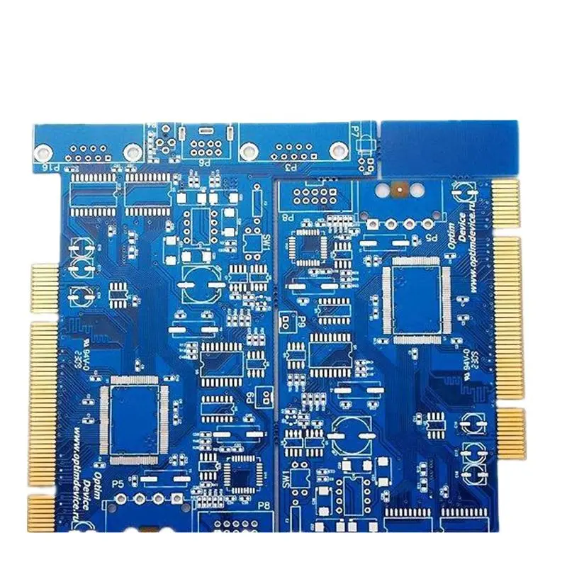
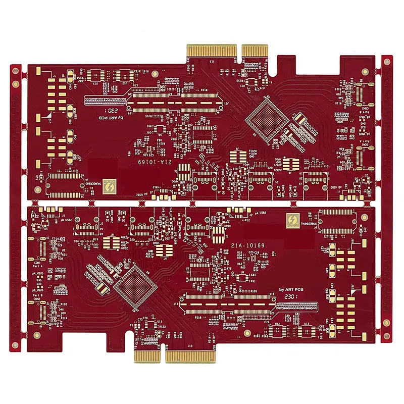
The board is constructed as a 10‑layer multilayer PCB, providing the necessary real estate for complex routing, dedicated power planes, and ground planes. This stack‑up is essential for managing electromagnetic interference (EMI) and providing a stable reference for controlled impedance signals.
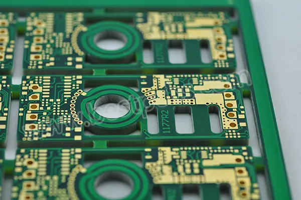
The final product has a finished thickness of 1.6 mm, a standard and mechanically robust thickness that ensures compatibility with industry‑standard connectors and enclosures. The copper thickness for both inner and outer layers is standardized at 1 oz (35 µm) , providing a balance between current‑carrying capacity and fine‑line etching capabilities.
Achieving high signal integrity requires precise control over conductor geometry. This board pushes manufacturing capabilities with a minimum trace width and spacing of 3 mils (0.075 mm) . This high level of precision is necessary to achieve the target characteristic impedance (typically 50 Ω or 100 Ω differential) and to accommodate the dense interconnect routing of modern system‑on‑chips (SoCs) and communication processors.
The chosen surface finish is Electroless Nickel Immersion Gold (ENIG) , with a gold thickness of 2 µ". ENIG is the industry‑preferred finish for communication PCBs for several reasons:
Flat Surface: Essential for the reliable soldering of fine‑pitch components like BGAs and QFNs.
Excellent Oxidation Resistance: Provides a long shelf life.
Reliable Solderability: The nickel barrier prevents copper migration, ensuring strong solder joints.
Ideal for Gold Wire Bonding: Should the application require it.
The defining characteristic of this PCB, as noted in the specification, is the requirement for high‑precision impedance control. In high‑frequency digital communication, signals are effectively radio frequency (RF) waves traveling along conductors. If the impedance of the PCB trace is not meticulously controlled and matched to the source and load, signal reflections occur, leading to data corruption, jitter, and system failure.
To achieve this, the manufacturing process involves:
Pre‑Stackup Simulation: Using field solvers to calculate the precise trace geometry required for the target impedance, considering the dielectric thickness and material properties.
Controlled Etching: Tightly managing the etching process to ensure the final trace cross‑section matches the simulated design.
Electrical Testing: Performing post‑production testing on coupon structures to verify that the impedance values are within the specified tolerance (e.g., ±10% ).
This combination of advanced materials, precise manufacturing tolerances, and impedance control makes this 10‑layer PCB ideal for a range of critical communication instruments, including:
Network analyzers and signal generators
Base station monitoring equipment
High‑speed data acquisition systems
Telecommunication infrastructure hardware
The manufacturing of a PCB for high‑frequency communication instruments is a discipline that blends material science with precision engineering. By selecting a high‑performance laminate like TU‑768, adhering to tight 3‑mil trace/space tolerances, applying a reliable ENIG finish, and enforcing rigorous impedance control protocols, manufacturers can produce PCBs that meet the stringent demands of modern communication technology. This technical approach ensures the signal integrity and reliability that these critical systems require.