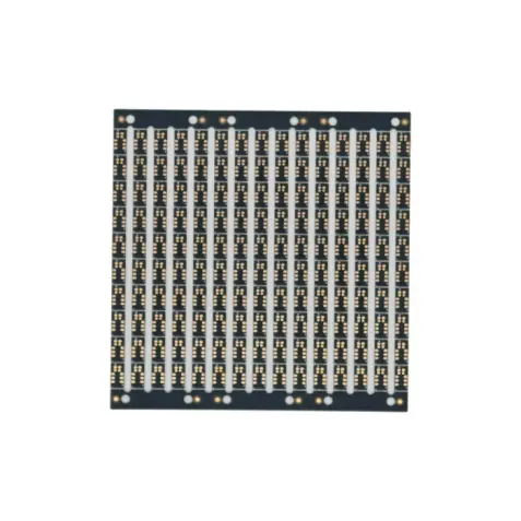
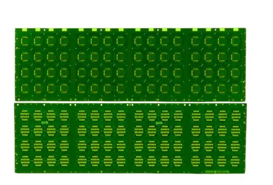
Technical Specifications and Manufacturing Insights for an 8-Layer Blind Via IC Substrate
In the realm of advanced electronics, the demand for higher performance in smaller form factors drives the need for sophisticated printed circuit board (PCB) technologies. Integrated Circuit (IC) substrates, particularly those utilizing High-Density Interconnect (HDI) processes like blind vias, are at the forefront of this innovation. This article provides a detailed technical examination of a specific 8-layer Blind Via IC Substrate, highlighting its key specifications and manufacturing significance.
Core Technical Data Analysis
"The substrate in question represents a high-end solution designed for demanding applications. Its specifications are detailed below:
1、Product Type: Blind Via IC Substrate
2、Construction: 8-Layer HDI Build-Up
3、Overall Thickness: 0.6 mm (±10%)
4、Panel Unit Dimensions: 40 mm x 55 mm
5、Dielectric Material: Mitsubishi Gas Chemical HF BT HL832NX. This high-frequency, halogen-free laminate is selected for its excellent thermal reliability, low dielectric loss, and superior electrical properties, which are critical for signal integrity in high-speed applications.
6、Minimum Laser Drilled Via Diameter: 0.1 mm (100 µm). This specifies the size of the microvias that form the blind connections between layers, a key enabler for HDI density.
7、Fine-Line Fabrication Capability: Minimum Trace Width / Space: 30 µm / 30 µm. This exceptionally fine patterning is essential for routing high-pin-count chips like BGAs and CSPs.
8、Solder Mask: PSR-4000 AUS308. This is a common photoimageable solder resist known for its high resolution and reliability, preventing solder bridges during component assembly.
9、Surface Finish: Soft Gold (Electroless Nickel Immersion Gold - ENIG). This finish provides a flat, solderable surface with excellent oxidation resistance, ideal for wire bonding and reliable solder joints."
Manufacturing and Design Significance
The combination of these specifications points to a substrate designed for high-performance computing, telecommunications, and advanced IC packaging.
1. HDI and Blind Vias: The use of blind vias (which connect an outer layer to one or more inner layers but do not go through the entire board) is a hallmark of HDI design. This allows for a higher density of interconnections in a smaller area, freeing up valuable real estate on inner layers for power and ground planes. The 0.1mm laser drill capability is a standard for modern HDI processes.
2. Material Selection: The choice of Mitsubishi's HL832NX material indicates an application that may involve high-speed digital or RF signals. Its properties help maintain signal integrity by minimizing loss and providing a stable electrical environment across a range of temperatures.
3. Fine-Line Patterning: Achieving a consistent 30µm line and space is a benchmark of advanced PCB fabrication. This capability is non-negotiable for substrates that interface with modern semiconductor packages, where pitch sizes continue to shrink.
4. Robust Finish and Mask: The specified solder mask and soft gold finish ensure long-term reliability and manufacturability, protecting the delicate copper traces from environmental factors and providing a optimal surface for the subsequent assembly processes.
Primary Applications
This Blind Via IC Substrate is engineered for applications requiring miniaturization and high electrical performance, such as:
Advanced IC Packaging: Including System-in-Package (SiP) and Package-on-Package (PoP).
High-Performance Computing (HPC) and Servers.
5G Network Infrastructure and RF Modules.
Medical Imaging and Diagnostic Equipment.
The detailed technical data of this 8-layer Blind Via IC Substrate underscores the advanced capabilities of modern PCB manufacturing. With its high-performance material, fine-line geometry, and HDI architecture, it serves as a critical enabling technology for the next generation of compact, powerful, and reliable electronic devices. Understanding these specifications is vital for engineers and designers working on the cutting edge of electronics.
Model: Blind Via IC Substrate
Base Material: Mitsubishi Gas HF BT HL832NX
Layer Count: 8-Layer Construction
Board Thickness: 0.6 mm
Unit Dimensions: 40 mm x 55 mm
Solder Mask: PSR-4000 AUS308
Surface Finish: Soft Gold
Minimum Laser Drill Aperture: 0.1 mm
Minimum Trace/Space: 30 µm / 30 µm
Primary Application: High-Density Interconnect (HDI) IC Substrate with Blind Vias