Technical Overview of a High-Density USB 3.0 PCB Substrate
The printed circuit board (PCB) is the fundamental platform upon which modern electronics are built. For high-speed data interfaces like USB 3.0, the substrate's design and manufacturing quality are paramount to ensuring signal integrity, reliability, and performance. This article provides a detailed technical examination of a specialized USB 3.0 PCB substrate, breaking down its key specifications and the manufacturing expertise required for its production.
Key Technical Specifications and Manufacturing Analysis
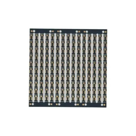
1. Board Definition and ApplicationThis substrate is explicitly engineered as a USB 3.0 PCB Substrate Board. Its primary function is to facilitate the high-speed data transfer rates (up to 5 Gbps) of the USB 3.0 standard, making it suitable for a range of applications, from external storage enclosures to high-performance peripherals.
2. Base Material: SI10UThe core material is specified as SI10U, a high-grade copper-clad laminate (CCL). This material is selected for its excellent electrical properties, thermal stability, and mechanical strength, which are critical for maintaining the integrity of high-frequency signals.
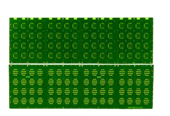
3. Multilayer Construction: 4-Layer (4L) DesignThe 4-layer stack-up is a common configuration for USB 3.0 boards. This architecture typically dedicates internal layers to power and ground planes, which provides effective shielding, reduces electromagnetic interference (EMI), and offers a stable return path for high-speed signals routed on the outer layers.
4. Precision Dimensional Tolerances
Board Thickness: The substrate features an ultra-thin profile of 0.3 mm. This slim form factor is essential for compact and lightweight device designs.
Outline Dimensions: The board's precise dimensions are 12.8 mm x 38.8 mm, indicating a specialized form factor tailored for a specific product or connector interface.
5. Surface Finish: Soft Gold (Electroless Nickel Immersion Gold - ENIG)The Soft Gold surface finish is a critical specification, professionally known as ENIG. This finish provides:
Excellent Surface Planarity: Crucial for the reliable soldering of fine-pitch components.
Good Oxidation Resistance: Ensures long-term solderability.
Superior Contact Surface: Ideal for connector pads and gold finger interfaces.
6. Solder Mask: PSR-2000 BL500The PSR-2000 BL500 refers to a specific, high-performance liquid photoimageable solder mask (LPI) in the color blue (BL500). This mask insulates the copper traces, preventing solder bridges and protecting the circuit from environmental damage.
7. Advanced Fabrication CapabilitiesThe listed minimum tolerances demonstrate a requirement for high-precision manufacturing processes:
Minimum Aperture (Drill Size): 0.1 mm - Indicates the use of micro-drilling technology for creating very small vias.
Minimum Conductor Width (Line Width): 40 µm - Reflects the ability to create extremely fine traces.
Minimum Conductor Spacing (Line Distance): 75 µm - Shows a high level of control over the etching process to prevent short circuits between dense traces. These tight tolerances are essential for the dense routing required by high-speed differential pairs in USB 3.0.
The specifications of this USB 3.0 PCB substrate board highlight the intersection of advanced materials engineering and precision manufacturing. The combination of the SI10U base material, a 4-layer construction, an ENIG surface finish, and exceptionally tight fabrication tolerances results in a substrate capable of supporting the demanding electrical requirements of high-speed data transmission. For engineers and procurement specialists, understanding these details is crucial for selecting a PCB manufacturer capable of delivering the quality and reliability necessary for high-performance consumer and industrial electronics.
Model: USB 3.0 PCB Substrate Board
Base Material: SI10U
Layer Count: 4L
Board Thickness: 0.3 mm
Outline Dimensions: 12.8 mm x 38.8 mm
Solder Mask: PSR-2000 BL500
Surface Finish: Soft Gold
Minimum Fabrication Tolerances: Drilled Hole Aperture: 0.1 mm
Conductor Spacing (Line Distance): 75 µm
Conductor Width (Line Width): 40 µm
Application: USB 3.0 PCB Substrate Board