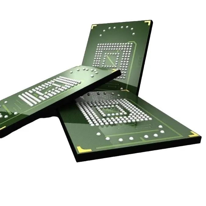
The evolution of modern electronics demands printed circuit boards (PCBs) that offer exceptional precision, reliability, and performance, especially when used as a core substrate for sophisticated components. This technical article provides a detailed examination of a specialized Component Substrate PCB engineered to meet these rigorous demands.
This substrate is characterized by its advanced material selection and fine‑line fabrication capabilities, making it suitable for high‑frequency or miniaturized devices. The critical parameters are as follows:
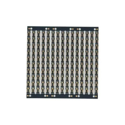
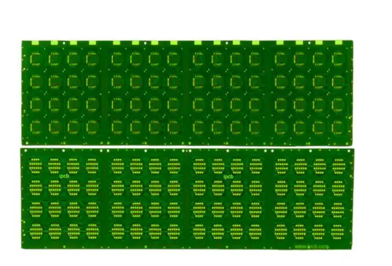
Construction and Materials: The board features a 2‑layer construction utilizing CC‑HL820WDI as the base laminate. This material is known for excellent thermal reliability and electrical properties, providing a stable foundation for the circuit.
Board Profile and Durability: A remarkably thin overall thickness of 0.3 mm is achieved, which is critical for applications where space constraints are paramount. The surface is protected by PSR‑4000 WT03 solder resist, ensuring insulation and resistance to environmental factors.
High‑Reliability Surface Finish: The critical contact surfaces are finished with an Electrolytic Hard Gold treatment. This finish offers superior wear resistance, excellent conductivity, and stable solderability over time, which is vital for the long‑term reliability of interconnects.
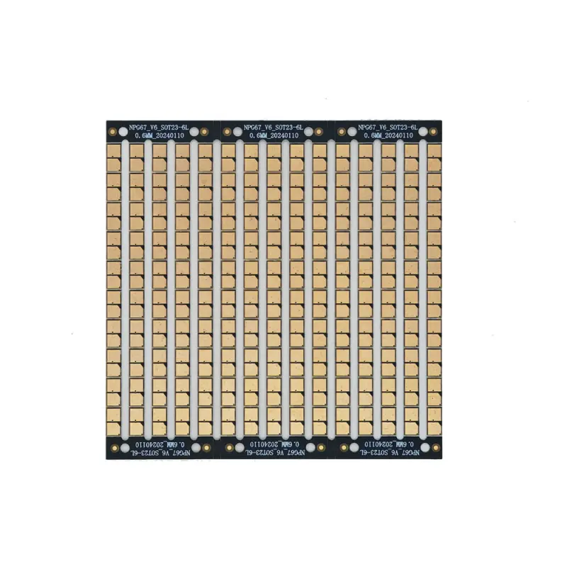
Precision Fabrication Tolerances: The manufacturing process demonstrates high precision, capable of achieving a minimum drill aperture of 0.25 mm and ultra‑fine trace width and spacing of 75 micrometers (µm) . These tight tolerances enable high circuit density and stable signal transmission.
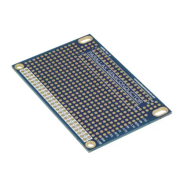
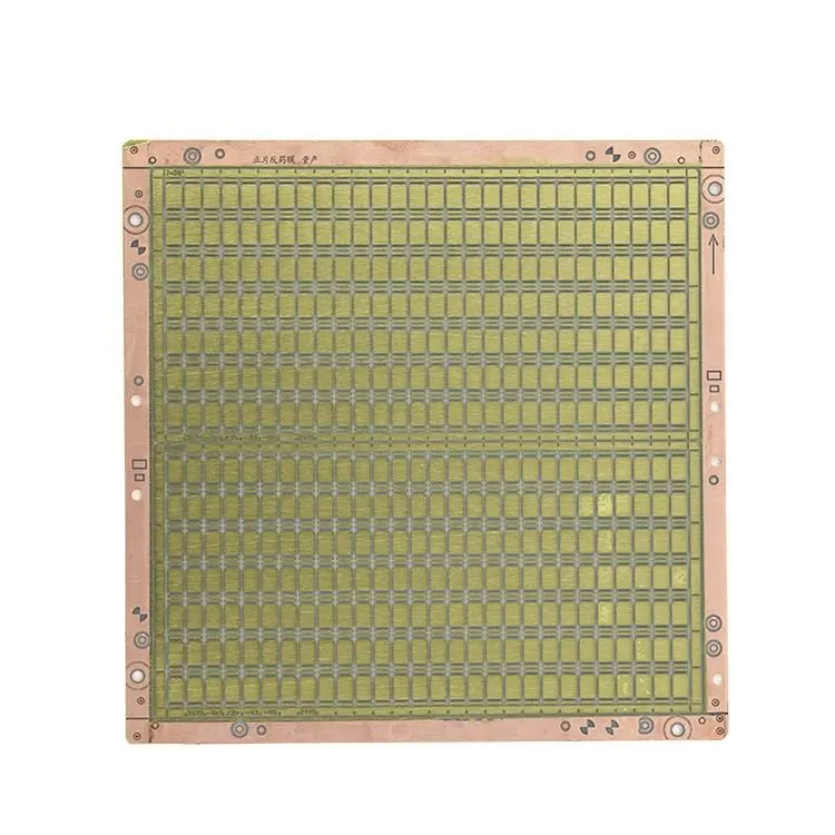
Primary Application: This PCB is explicitly designed for use as an Electronic Components Substrate, indicating its role as a foundational element within complex integrated circuits, system‑in‑package (SiP) modules, or other advanced semiconductor packaging.
The combination of these specifications results in a substrate with several key advantages:
Signal Integrity: The fine line geometry and controlled impedance of the base material contribute to enhanced signal integrity at high frequencies.
Miniaturization Potential: The thin profile and high wiring density directly support the ongoing trend towards smaller and more powerful electronic devices.
Robust Performance: The hard gold plating ensures durable and oxidation‑resistant contact points, which is crucial for components requiring repeated mating or operation in challenging environments.
In conclusion, this Component Substrate PCB represents a high‑performance solution tailored for the core of advanced electronic systems. Its specifications reflect a focus on precision, reliability, and miniaturization, making it an ideal choice for engineers designing cutting‑edge technology in telecommunications, computing, and consumer electronics.