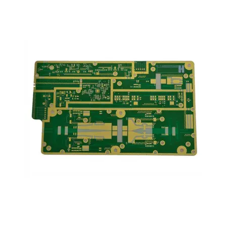
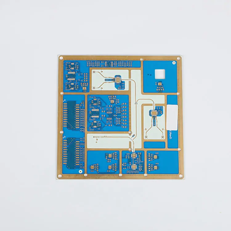
Cavity PCBs represent a sophisticated segment of printed circuit board technology, essential for advanced radio frequency (RF) and microwave systems. This article provides a detailed technical examination of a specific Cavity PCB engineered for a power divider application, analyzing its material selection, critical performance parameters, and the manufacturing considerations implied by its specifications.
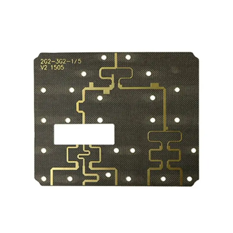
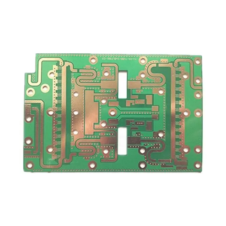
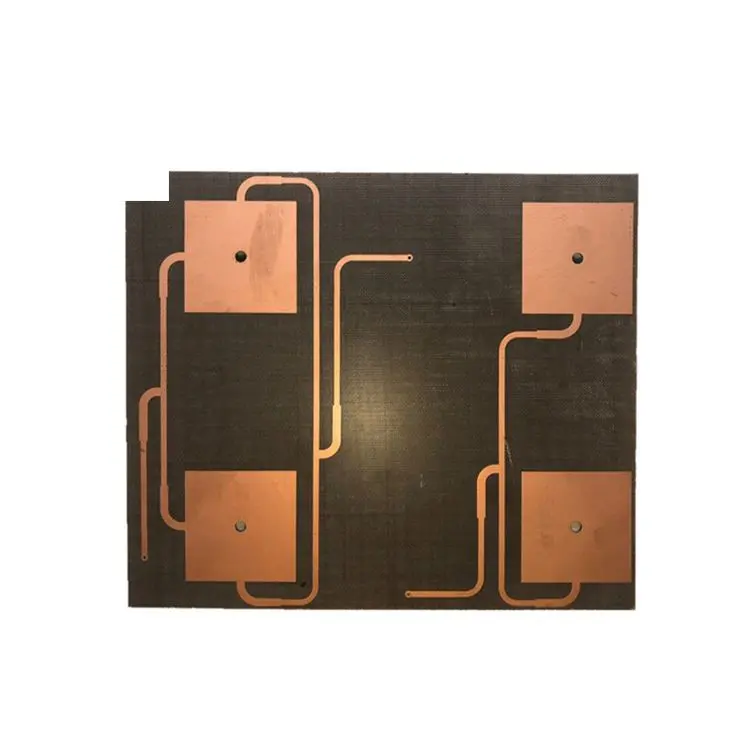
A Cavity PCB incorporates precisely milled recesses (cavities) within the board substrate to accommodate components or to create specific electromagnetic environments. This design eliminates the need for surface mounting of certain components, reducing the overall profile (z‑height) and improving high‑frequency signal integrity by minimizing parasitic effects. The board in review is designated explicitly for a power divider, a critical component used to split an input signal into multiple output signals with controlled phase and amplitude.
The core material of this board is specified as Teflon F4MB, a ceramic‑filled polytetrafluoroethylene (PTFE) composite. This choice is strategic for high‑performance applications due to its exceptional properties:
Stable Dielectric Constant (Dk): The specified Dk of 2.55 is low and highly stable over a wide frequency range, which is crucial for predictable signal propagation velocity and impedance control.
Low Dissipation Factor (Df): PTFE exhibits minimal signal loss (attenuation), making it ideal for sensitive RF circuits where signal integrity is paramount.
Excellent Thermal Stability: F4MB maintains its electrical and mechanical properties across varying temperatures, ensuring consistent performance of the power divider.
The provided datasheet outlines key parameters that define the board's capabilities and the required manufacturing precision:
Quality Standard: Conformance to IPC‑6012 Class 2 ensures a high degree of reliability suitable for commercial and industrial electronic products where extended life and performance consistency are required.
Layer Construction: This is a 2‑layer board, indicating a relatively simple stack‑up. The complexity lies not in the layer count but in the cavity creation process.
Board Thickness: The final thickness of 1.5 mm provides a robust mechanical structure while allowing for the necessary cavity depth.
Controlled Impedance and Copper Thickness: The use of 0.5 oz base copper with a final finished thickness of 1 oz suggests a plating process that builds up the copper in the through‑holes and on the surface. This is critical for achieving the current‑carrying capacity and consistent impedance needed for the power divider's transmission lines.
Surface Finish: Immersion Silver (Imm‑Ag) . This finish was selected for its excellent surface planarity (flatness), which is beneficial for high‑frequency signals, and its good solderability. It provides a reliable surface for assembly while being more cost‑effective than finishes like gold for certain applications.
The creation of the cavity is a precision machining operation, typically performed using computer‑controlled routing or milling machines. Key considerations in this process include:
Depth Control: The cavity depth must be held to tight tolerances to ensure components sit correctly and electrical performance meets design goals.
Wall Plating: Depending on the design, the cavity walls may need to be metallized (plated) to form a shielded compartment or to create specific electrical connections within the board.
Material Handling: Machining PTFE requires specialized tools and techniques to prevent material tearing or deformation, ensuring clean and precise cavity edges.
The specified Cavity PCB—with its PTFE/F4MB substrate, controlled dielectric properties, immersion silver finish, and adherence to IPC‑6012 Class 2—is a purpose‑built solution for demanding RF applications like power dividers. Its design reflects a careful balance of high‑frequency performance, manufacturability, and reliability. Understanding these specifications is vital for engineers designing systems where signal integrity and integration density are critical.