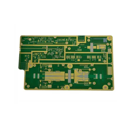
Radar systems demand unparalleled performance and reliability from their core components, with the Printed Circuit Board (PCB) being fundamental to their operation. Success in applications ranging from automotive collision avoidance to aerospace and defense sensing hinges on the precise electrical and mechanical characteristics of the PCB. This technical article outlines the critical manufacturing specifications for advanced Radar PCBs engineered for high‑frequency applications.
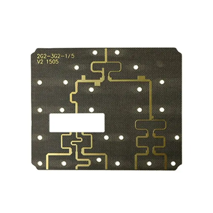
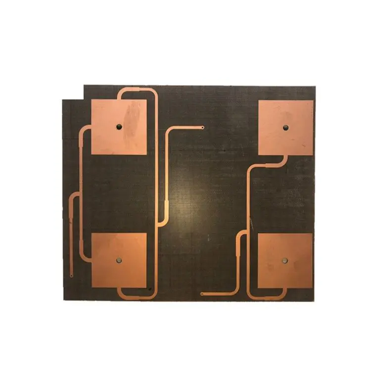
The foundation of any high‑performance Radar PCB is its substrate material. Our boards utilize advanced materials such as Polytetrafluoroethylene (PTFE/Teflon) and ceramic‑filled composites. These materials are selected for their superior high‑frequency properties, including:
Low Loss Tangent: Minimizes signal loss at radar frequencies (e.g., 24 GHz, 77 GHz, and beyond).
Stable Dielectric Constant (Dk): Ensures consistent signal integrity. The available Dk range of 2.0 to 16.0 allows for impedance matching and design flexibility to meet specific system requirements.
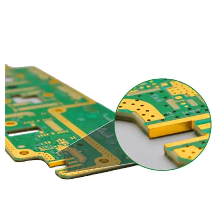
Quality and reliability are non‑negotiable. Our Radar PCB manufacturing process strictly adheres to the IPC‑6012 Class 2/3 standard for qualification and performance of rigid PCBs. This certification guarantees that every board meets the highest industry benchmarks for acceptability, including stringent criteria for conductor spacing, plating quality, and laminate integrity.
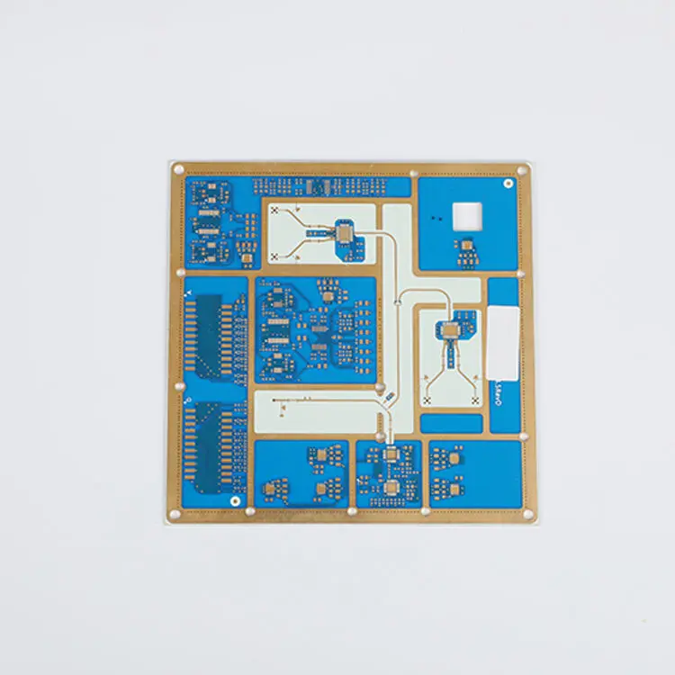
To support complex radar architectures—from simple transceiver modules to sophisticated array systems—we offer extensive design flexibility:
Layer Count: Configurations ranging from single‑layer to highly complex 70‑layer stack‑ups.
Board Thickness: Precision thickness control, with options from a thin 0.254 mm (10 mils) to a robust 6.0 mm, accommodating various form factors and mechanical constraints.
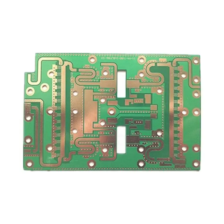
Signal integrity is paramount. We maintain consistent 1 oz finished copper thickness (H/H oz) for inner and outer layers, which is critical for achieving controlled impedance. This, combined with our material expertise, ensures minimal signal distortion and optimal power delivery.
The choice of surface finish impacts assembly yield and long‑term reliability. The primary finish we recommend is Immersion Silver, chosen for its excellent surface planarity and solderability. Alternative finishes, including Electroless Nickel Immersion Gold (ENIG) and Organic Solderability Preservative (OSP) , are available to suit specific assembly processes and environmental requirements.
These high‑specification PCBs are designed for critical applications in:
Communication Radar Systems
Detection and Sensing Radar Systems
Manufacturing PCBs for modern radar technology requires a deep understanding of high‑frequency electronics and precision engineering. By specifying materials like Teflon and ceramic, adhering to IPC‑6012, and offering a wide range of configurable parameters, we provide the robust foundation necessary for the next generation of communication and detection radar systems. For engineers designing critical sensing applications, these specifications represent a benchmark for performance and reliability.