Technical Specifications and Applications of the Kevis A4009 High-Performance Ceramic PCB
In the demanding fields of modern electronics, the choice of printed circuit board (PCB) is critical to the performance, reliability, and longevity of the final product. The Kevis A4009 ceramic PCB represents a premium solution engineered for applications where standard FR-4 substrates fall short. This technical data sheet provides a detailed overview of its specifications and ideal use cases.
Product Overview
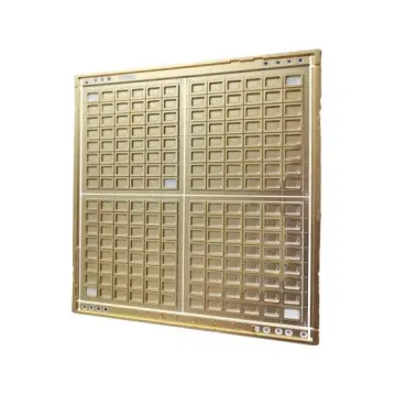
The A4009 is a ceramic-based circuit board manufactured by Kevis in Guangdong, China, a hub for advanced electronics production. Ceramic PCBs are renowned for their superior thermal conductivity, excellent high-frequency performance, and robust mechanical stability compared to traditional materials. This model is offered as part of a comprehensive "One-Stop PCB Assembly Service," streamlining the transition from design to finished product.
"Key Technical Specifications
Panel Size: 109.2 mm x 109.2 mm / 170 mm x 60 mm. This offers flexibility for manufacturing arrays of smaller boards or producing specific form factors.
Model Number: PCB A4009.
Type: Ceramic PCB (Ceramic Substrate).
Copper Thickness: 65 ±15 µm. This standardized thickness ensures consistent current-carrying capacity and signal integrity.
Minimum Hole Diameter: ≥ 0.25 mm. This specification defines the capability for creating vias and through-hole component placements.
Minimum Line Width / Spacing: The A4009 supports high-density interconnects (HDI) with a minimum line width of ≥ 0.12 mm and a minimum line spacing of ≥ 0.1 mm for gold surfaces and > 0.08 mm for silver surfaces. These tight tolerances are essential for complex, miniaturized designs. "
Advanced Surface Finish Options
"To meet diverse application requirements, the A4009 is available with a range of high-quality surface finishes:
1、Immersion Silver (Ag): Provides a flat surface for solderability and is cost-effective.
2、Nickel-Silver (NiAg): Offers a durable, solderable surface.
3、Electroless Nickel Immersion Gold (ENIG/ NiAu): The industry standard for fine-pitch components, offering a flat surface, excellent oxidation resistance, and good solderability.
4、Nickel-Palladium-Gold (NiPdAu): A premium finish known for superior wire bonding capability and long-term reliability.
5、Electroplated Nickel-Gold: Offers a thick, durable gold layer for edge connectors and harsh environments."
Primary Application Fields
"The combination of a ceramic substrate and precise manufacturing makes the Kevis A4009 PCB ideally suited for:
Industrial Controls: Withstands harsh environments, high temperatures, and vibrations found in factory automation and control systems.
Medical Electronics: Offers the reliability and stability required for sensitive diagnostic and therapeutic equipment.
Energy Storage Systems (ESS): Excellent thermal management is crucial for battery management systems (BMS) in renewable energy and EV applications.
Communication Equipment: The superior high-frequency characteristics of ceramic make it ideal for RF and microwave communication devices."
The Kevis A4009 Ceramic PCB is a high-specification component designed for engineers seeking maximum performance and reliability. Its robust construction, fine-line capabilities, and range of surface finishes make it a versatile choice for next-generation electronic products across critical industries. For detailed design guidelines, DFM rules, or to discuss your specific project needs within our one-stop assembly service, please contact our technical sales team.
Panel Size: 109.2 * 109.2mm / 170 * 60mm
Copper Thickness: 65±15 µm
Minimum Hole Diameter: ≥ 0.25mm
Minimum Line Width: ≥ 0.12mm
Minimum Line Spacing: ≥ 0.1mm (Au) / > 0.08mm (Ag)
Surface Finish: Immersion Silver (Ag), Nickel-Silver (NiAg), Electroless Nickel Immersion Gold (ENIG/NiAu), Nickel-Palladium-Gold (NiPdAu), Electroplated Nickel-Gold
Application Fields: Industrial Controls, Medical, Energy Storage, Communications