Technical Overview of a High-Density Component Substrate PCB
In the realm of advanced electronics manufacturing, the substrate forms the critical foundation upon which component performance and reliability are built. This article provides a detailed technical examination of a specialized Component Substrate PCB, analyzing its key specifications and their implications for design and manufacturing.
Core Construction and Material Selection
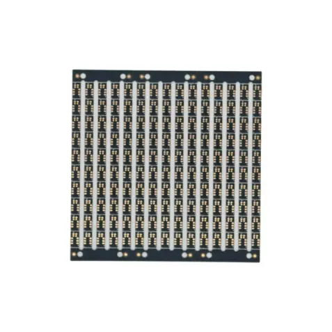
The substrate in question is a 2-layer printed circuit board characterized by an ultra-thin profile. The base material, identified as CC-HL820WDI, is a high-performance laminate likely formulated for excellent thermal stability and electrical properties. This material choice is paramount for applications requiring consistent performance.
A standout feature of this board is its 0.3mm finished thickness. This ultra-thin construction is essential for applications where space and weight are at a premium, such as in miniaturized consumer electronics, compact sensors, and advanced packaging.
Precision Fabrication and Surface Finishes
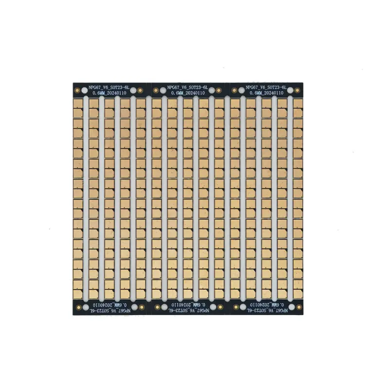
The manufacturing tolerances of this substrate indicate its use in high-precision applications. The design incorporates a minimum via diameter of 0.25mm, facilitating reliable interlayer connections. Furthermore, the board features a minimum line width and spacing of 75µm (microns). This fine-line geometry is indicative of a high-density interconnect (HDI) capability, allowing for a greater number of circuits in a confined area.
For surface protection and solderability, the board utilizes PSR-4000 WT03 solder mask. The "WT" designation typically signifies a white color, often used for improved contrast or for applications like LED packaging where reflectivity is beneficial. The final surface finish is specified as Hard Gold. This finish offers superior wear resistance, excellent corrosion resistance, and stable contact resistance, making it ideal for connector pads, gold finger contacts, and areas subject to frequent mating or harsh environment
Primary Application and Conclusion
As explicitly defined, the primary application of this PCB is as a substrate for electronic components. This broad term encompasses its potential use as a base for complex integrated circuits (ICs), multi-chip modules (MCMs), or other semiconductor packages. The combination of a thin core, high-quality material, hard gold plating, and fine-line patterning makes it a robust and reliable solution for demanding electronic packaging.
In summary, the technical specifications of this Component Substrate PCB point to a product engineered for high reliability and miniaturization. Its thin profile, fine features, and durable surface finish make it a suitable choice for advanced electronic applications where performance and space constraints are critical design factors.
Product Model: CC-HL820WDI
Base Material: Component Substrate PCB
Layer Count: 2 layers
Board Thickness: 0.3 mm
Solder Mask: PSR-4000 WT03
Surface Finish: Hard Gold Plating
Minimum Via Diameter: 0.25 mm
Minimum Line Spacing: 75 µm
Minimum Line Width: 75 µm
Primary Application: Substrate for Electronic Components