The core of a reliable fingerprint recognition system lies in its integrated circuit (IC), which requires a sophisticated and high‑performance package substrate to function optimally. This technical article details the specifications and manufacturing capabilities of a specialized IC package substrate engineered explicitly for fingerprint card applications. This substrate serves as the critical foundation, providing electrical interconnection, mechanical support, and environmental protection for the sensitive semiconductor die.
The substrate is built to meet the stringent demands of modern biometric security devices. Below is a breakdown of its critical parameters:
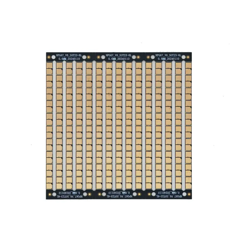
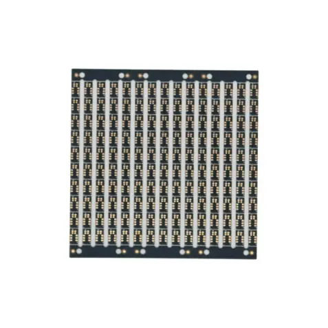
Model & Application: This substrate is designated for Fingerprint Card IC Package Substrate, highlighting its specialized role in biometric authentication modules.
Construction and Materials: The substrate utilizes a 2‑layer (2L) construction with Shengyi S110U as the primary dielectric laminate. This material is renowned for its excellent thermal stability, electrical properties, and suitability for high‑density interconnect (HDI) designs. The complete structure maintains an ultra‑thin overall thickness of 0.2 mm, which is crucial for the slim form factor of modern smart cards and mobile devices.
Dimensions: The unit features a compact single size of 11.0 mm x 11.0 mm, making it ideal for space‑constrained applications without compromising on functionality.
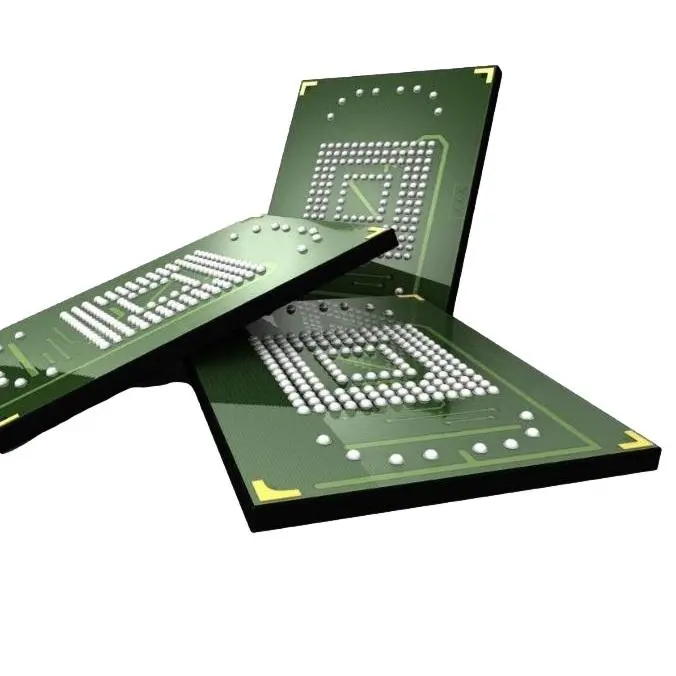
Surface Finish: The surface treatment employs Electroless Nickel Immersion Gold (ENIG) , combining a layer of Soft Gold for reliable wire bonding and Hard Gold for durable contact surfaces. This ENIG finish offers a flat surface for precise assembly and excellent oxidation resistance.
Solder Mask: The solder mask is specified as PSR‑4000 AU5306, a high‑resolution, photoimageable epoxy that protects the circuitry and ensures reliable solder pad definition.
Precision Manufacturing Capabilities: The substrate showcases advanced manufacturing precision, supporting a minimum laser via aperture of 0.1 mm. The circuitry is defined with a minimum line width/space (L/S) of 75 μm / 75 μm, and a minimum trace width of 35 μm. These tight tolerances are essential for accommodating the high I/O density of modern fingerprint sensor ICs.
The combination of these specifications makes this substrate an optimal solution for fingerprint cards:
Thin Profile & Small Outline: Allow for seamless integration into compact devices.
High‑Density Wiring Capabilities: Ensure flawless data transmission between the sensor IC and the main processor.
Robust ENIG Surface Treatment: Guarantees long‑term reliability and stable electrical performance—paramount for security‑focused biometric applications that require consistent accuracy over their lifespan.
This Fingerprint Card IC Package Substrate represents a precision‑engineered component tailored for the demanding biometric industry. Its 2L HDI design, ultra‑thin profile, and advanced ENIG surface finish meet the critical requirements for performance, reliability, and miniaturization. Manufacturers seeking a high‑quality foundation for their fingerprint recognition modules will find this substrate specification aligns perfectly with the needs of next‑generation security solutions.