Engineering High-Density FPGA PCBs: A Guide to Critical Manufacturing Specifications
The complexity of modern Field-Programmable Gate Arrays (FPGAs) demands an equally sophisticated approach to Printed Circuit Board (PCB) design and assembly. Selecting the right manufacturing specifications is paramount to ensuring signal integrity, power integrity, and long-term reliability in high-speed digital systems. This article details the essential technical parameters for a successful high-density FPGA PCB assembly project.
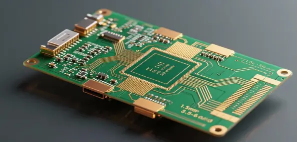
1. High-Density PCB Construction: Supporting up to 56 Layers
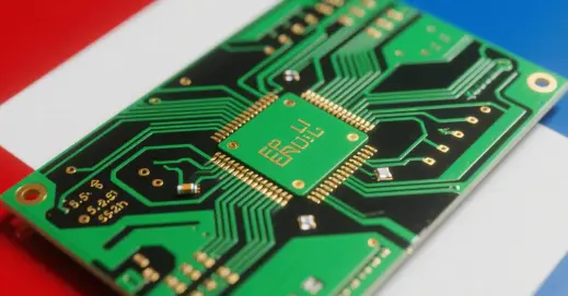
To accommodate the high pin-count and complex routing requirements of advanced FPGAs, PCB fabrication must support high-layer counts. A capability of up to 56 layers is indicative of a manufacturer equipped for sophisticated, multi-gigabit designs common in applications like data centers, telecommunications infrastructure, and high-performance computing. This allows for dedicated signal, power, and ground planes, which are critical for managing EMI and crosstalk.
2. Core Substrate Material: High-Tg FR-4
The foundation of any reliable PCB is its substrate material. The specification of FR-4 with a High Glass Transition Temperature (High-Tg) is essential for FPGA applications. High-Tg materials (typically >170°C) offer superior thermal and mechanical stability, preventing board deformation or delamination during the soldering process and ensuring performance under continuous operational thermal stress.
3. Superior Surface Finish: Electroless Nickel Immersion Gold (ENIG)
For the fine-pitch pads of FPGAs, a flat, reliable surface finish is non-negotiable. Electroless Nickel Immersion Gold (ENIG) is the industry-preferred choice. This finish provides a flat surface for excellent solderability, a robust nickel barrier between the copper and solder, and a thin gold layer that prevents oxidation. The specified gold thickness of 2 to 5 microinches (µ") offers an ideal balance between corrosion resistance and cost-effectiveness without risking solder joint embrittlement.
4. Controlled Impedance and Current Handling: Copper Thickness
The specified copper weight range of 0.5 oz/ft² to 2.0 oz/ft² provides design flexibility. Thinner copper (e.g., 0.5 oz) is ideal for fine-line signal traces where controlled impedance is critical. Thicker copper (e.g., 2.0 oz) is used for power planes to efficiently deliver high currents to the FPGA with minimal voltage drop and heating.
5. Solder Mask and Aesthetic Options
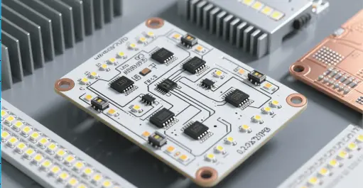
A Green Liquid Photoimageable (LPI) Solder Mask is the standard, offering excellent resolution for covering tight spaces between BGA pads. The availability of multiple PCB colors (Green, Black, White, Red, Blue) caters to both aesthetic branding and functional needs, such as using white for LED-based assemblies.
6. Mandatory Quality Assurance: PCB and PCBA Testing
The commitment to quality is explicitly confirmed with mandatory testing protocols.
PCB Testing (Yes): This verifies the bare board's integrity, ensuring no shorts or opens exist in the circuitry before components are assembled. Methods include flying probe or bed-of-nails testing.
PCBA Testing (Yes): After assembly, the board undergoes In-Circuit Test (ICT) and/or Functional Test to validate that all components are correctly placed, soldered, and operating as intended. This two-tiered testing approach is critical for achieving high first-pass yield and long-term field reliability for complex FPGA-based assemblies.
"Successfully manufacturing a PCB for a high-performance FPGA requires a deliberate selection of advanced materials and rigorous process controls. The specifications outlined here—from the high-layer count and High-Tg substrate to the ENIG finish and comprehensive testing—form a robust framework for developing reliable, cutting-edge electronic products. When sourcing your next FPGA PCB assembly, verifying these capabilities with your manufacturing partner is a critical step toward project success.
"
PCB Construction: Up to 56 layers
Substrate Material: FR-4, High Tg (High Glass Transition Temperature)
Surface Finish: Electroless Nickel Immersion Gold (ENIG)
Gold Thickness: 2 to 5 microinches (µ")
Solder Mask: Green LPI (Liquid Photoimageable)
Copper Weight: 0.5 oz/ft² to 2.0 oz/ft²
PCB Color Options: Green, Black, White, Red, Blue
PCB Test: Mandatory (e.g., Flying Probe/Test Coupon)
PCBA Test: Mandatory (In-Circuit Test / Functional Test)