Technical Specifications for Manufacturing High-Performance RF Communication PCBAs
The manufacturing of Printed Circuit Board Assemblies (PCBAs) for Radio Frequency (RF) communication systems demands rigorous attention to detail and specific material selections to ensure signal integrity, thermal management, and long-term reliability. The following technical outline details the key parameters for a standard 4-layer RF communication PCBA.
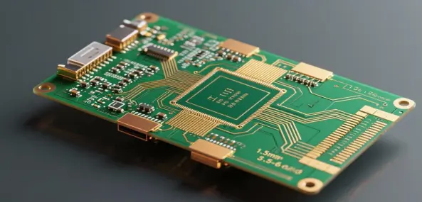
1. PCB Construction and Materials
Layer Count: This design utilizes a 4-layer board stack-up. This configuration is ideal for RF applications as it allows for a dedicated internal ground plane, which is critical for providing a stable reference and shielding against electromagnetic interference (EMI). A second internal layer is typically allocated for power, creating a clean and well-regulated power distribution network (PDN).
Substrate Material: The board is fabricated using a high-frequency or high-speed laminate. Unlike standard FR-4 materials, these specialized substrates are engineered with a low dielectric constant (Dk) and a low dissipation factor (Df). This minimizes signal loss and phase distortion at high frequencies, which is paramount for the performance of RF circuits.
Copper Thickness: The specification calls for external layer copper weights ranging from 0.5 oz to 6 oz, and internal layers from 0.5 oz to 5 oz. Thicker copper (e.g., 2 oz and above) is often selected for power amplifier sections to handle higher current loads and improve thermal dissipation.
2. Surface Finish and Solder Mask
Surface Finish: Two industry-standard finishes are offered:
Immersion Gold (ENIG): This is the preferred choice for most RF applications. It provides a flat, planar surface excellent for fine-pitch components and offers superior solderability and oxidation resistance. The specified gold thickness is 1 to 5 microinches (µ"), which protects the underlying nickel barrier during storage and before soldering.
HASL Lead-Free: A cost-effective alternative, Hot Air Solder Leveling provides a thick, reliable solderable coating. However, its uneven surface may not be suitable for very fine-pitch components.
Solder Resist: A standard green solder mask is applied to the board. This layer insulates the copper traces, prevents solder bridges during assembly, and provides the characteristic green color.
3. Quality Assurance and Testing
Robust testing is non-negotiable for RF PCBAs. This process includes:
100% PCB Electrical Testing: Each bare circuit board undergoes electrical testing to verify continuity (no open circuits) and isolation (no short circuits), ensuring the board is fabricated to the correct netlist.
Comprehensive PCBA Testing: After component assembly, the finished PCBA is subjected to a full suite of tests. This includes In-Circuit Test (ICT) to validate component value, orientation, and placement, as well as full functional testing to ensure the assembled board operates according to its RF performance specifications (e.g., gain, output power, noise figure).
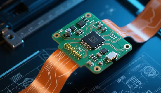
Application
These manufacturing specifications are specifically tailored for RF communication systems, including but not limited to wireless infrastructure, two-way radios, and various telecommunications equipment where stable high-frequency performance is critical.
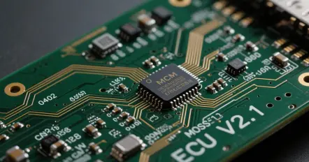
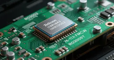
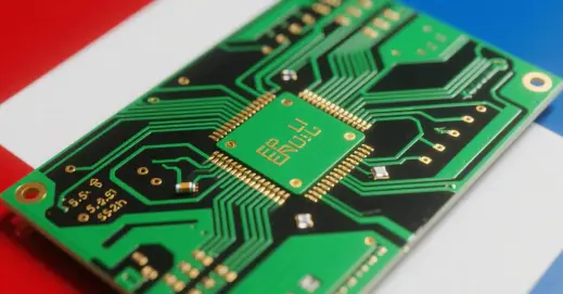
Board Construction: 4-Layer Printed Circuit Board
Substrate Material: High-Frequency/High-Speed Laminate
Surface Finish: Lead-Free Hot Air Solder Leveling (HASL) or Immersion Gold (ENIG)
Gold Thickness (ENIG): 1 to 5 Microinches (µ")
Solder Mask: Standard Green
Copper Thickness: 0.5 oz to 6 oz (External Layers); 0.5 oz to 5 oz (Internal Layers)
Quality Assurance: 100% PCB Electrical Testing & Full PCBA Functional/In-Circuit Testing (ICT)
Application: Designed for RF Communication Systems