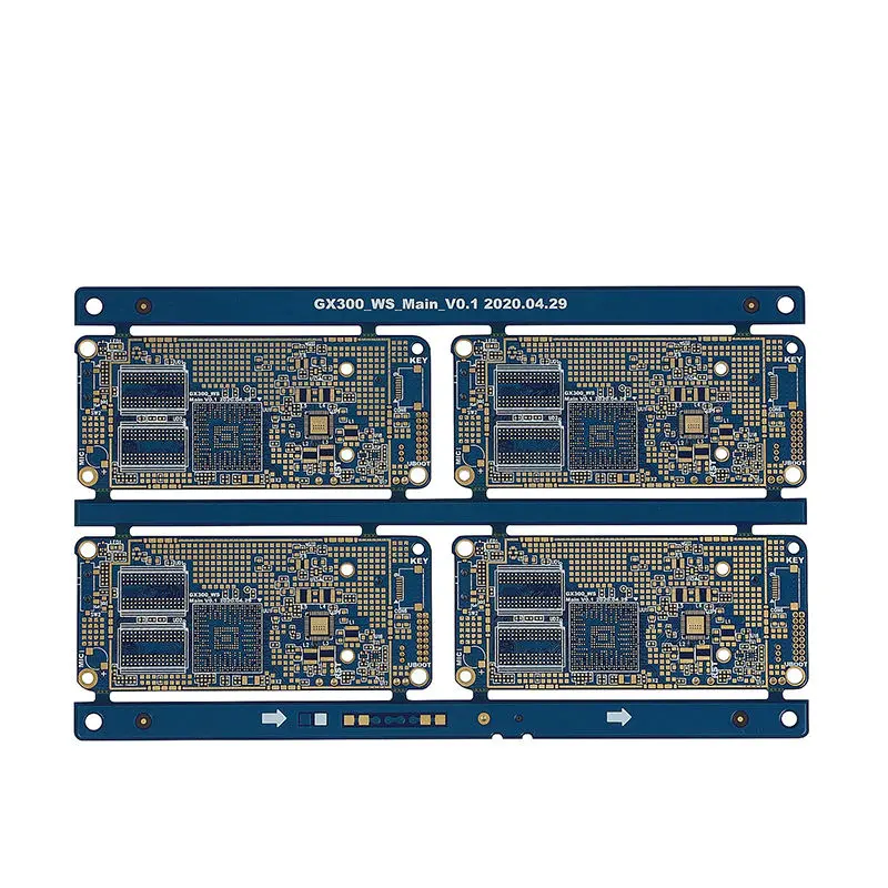
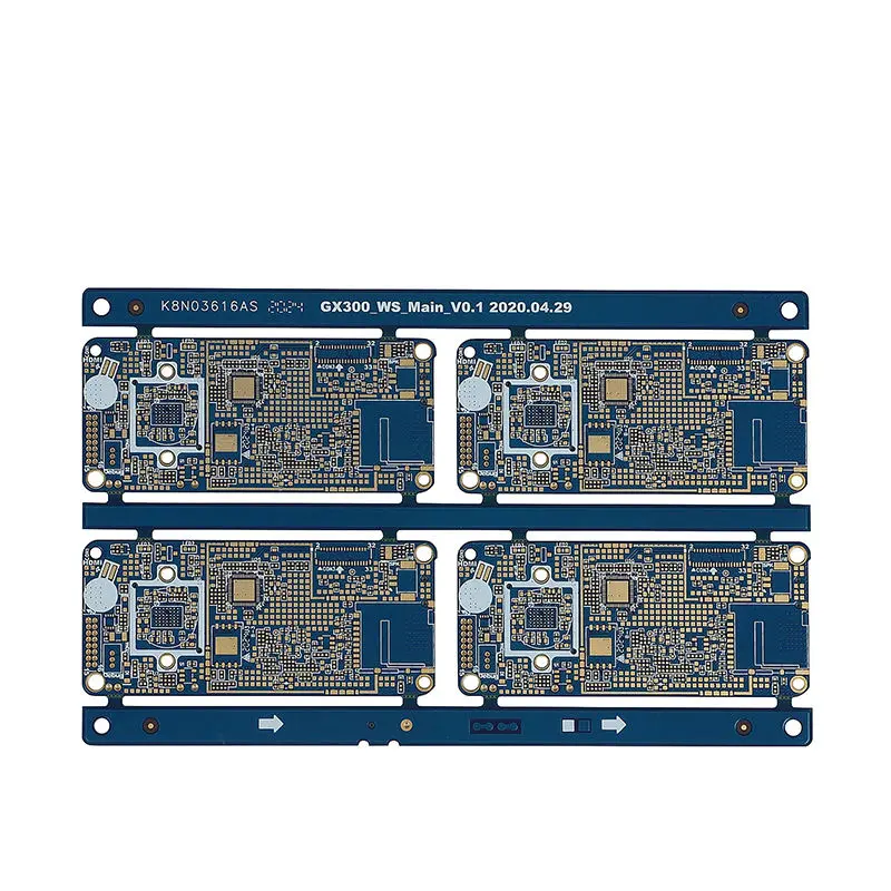
Technical Overview: A High-Density Interconnect (HDI) 10-Layer PCB with Mouse Bite Panelization
High-Density Interconnect (HDI) printed circuit boards represent the forefront of miniaturization and performance in the electronics industry. This technical article provides a detailed examination of a specific 10-Layer HDI PCB design that incorporates "mouse bite" panelization for efficient assembly. This board is engineered for complex consumer electronic devices where space constraints, signal integrity, and high reliability are critical design parameters. The following sections break down its key manufacturing specifications and their implications for performance.
Core Material and Construction
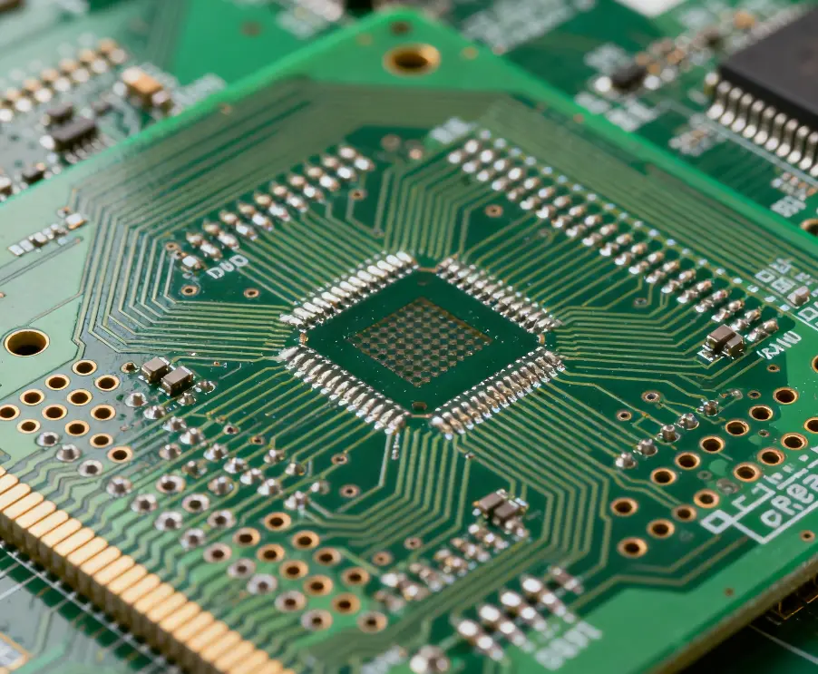
The foundation of this PCB is the high-performance SY S1000-2 laminate material, known for its excellent thermal stability and electrical properties, making it suitable for demanding applications. The board features a sophisticated 10-layer stack-up, configured in a 1+4+1 HDI build-up (the "q" in the original spec is interpreted as a typo for "1," indicating a sequential lamination process). This construction typically involves building up four core layers, with additional microvia layers on the top and bottom. This allows for a higher density of interconnections in a thinner profile.
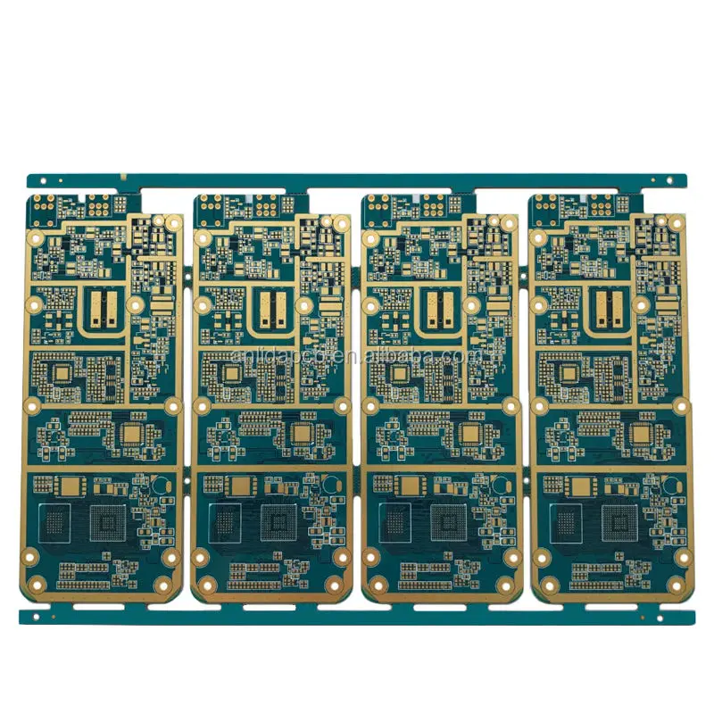
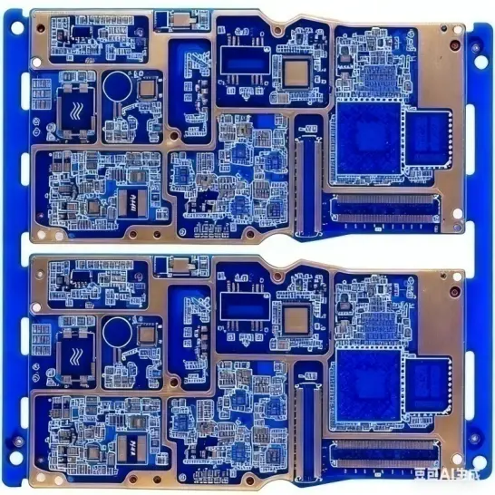
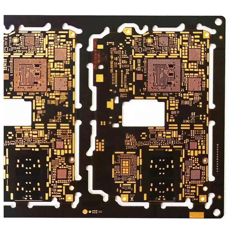
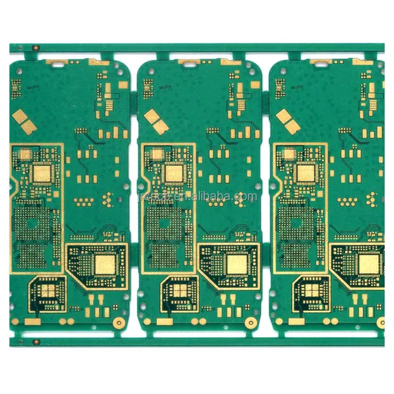
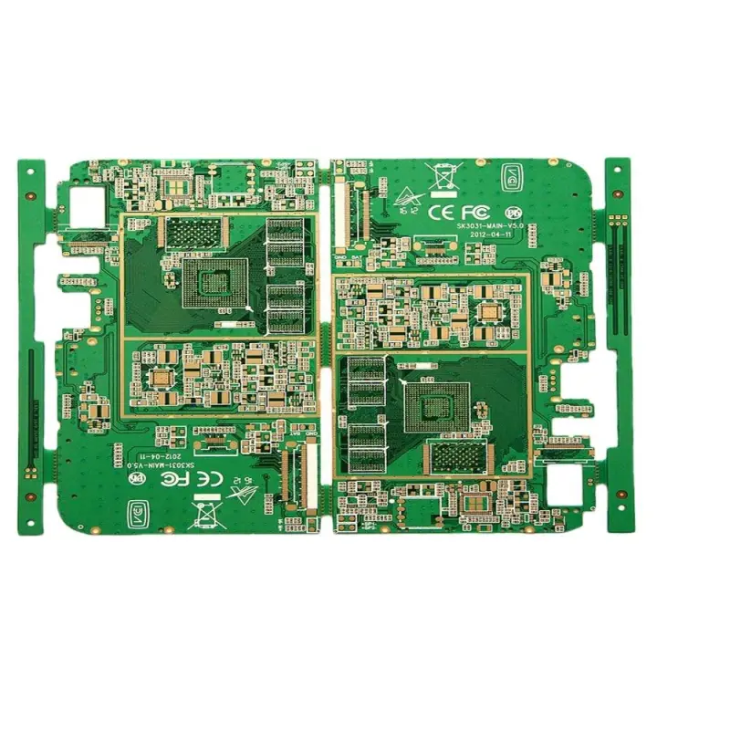
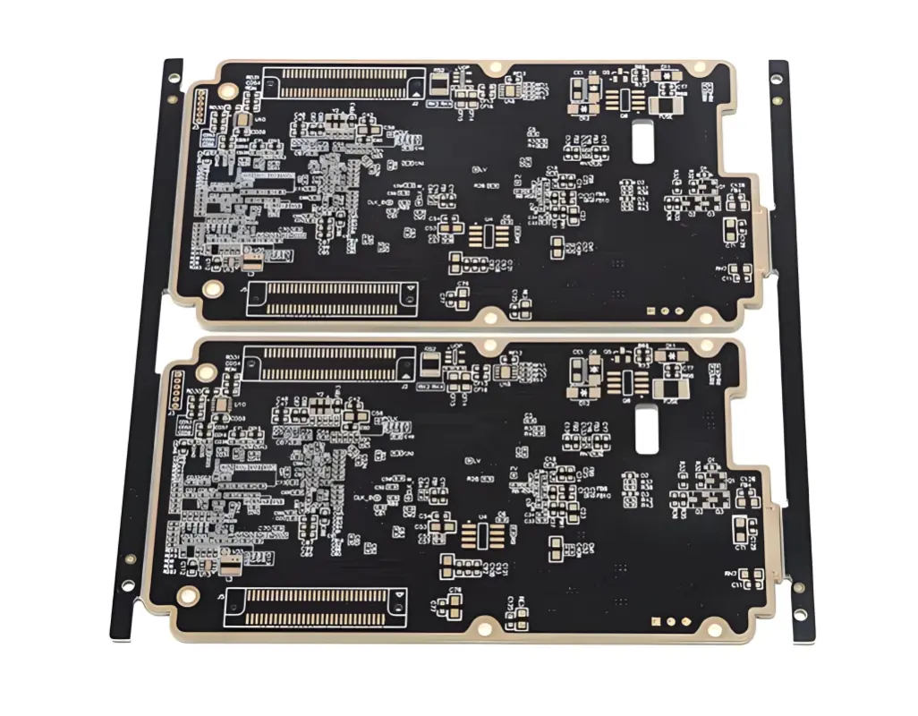
A critical feature of this design is the use of mouse bites—small, perforated tabs that secure the PCB within a larger panel during manufacturing. This method facilitates automated assembly and protects the delicate boards until they are depanelized for final use.
Key Physical and Electrical Specifications
1、Finished Thickness: The board is manufactured to an ultra-slim profile of 0.8mm, essential for compact, modern consumer gadgets like smartphones, advanced wearables, and miniaturized IoT modules.
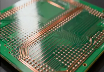
2、Copper Weight: A consistent 1 oz (ounce) copper thickness is applied on all internal and external layers. This standard weight provides an optimal balance for current-carrying capacity and fine-line etching.
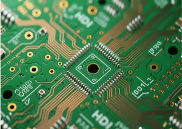
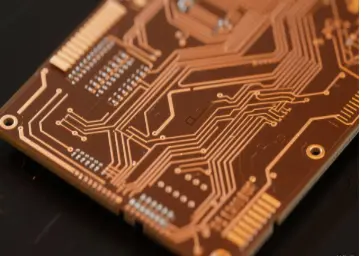
3、Minimum Trace/Space: The board supports a high-density design rule of 3 mil (0.003 inches) for both trace width and spacing. This level of precision is a hallmark of HDI technology, enabling complex routing for high-pin-count components like BGAs and microprocessors.
4、Surface Finish: The board utilizes Electroless Nickel Immersion Gold (ENIG) as its surface finish. ENIG offers a flat, durable surface ideal for fine-pitch components, provides excellent solderability, and protects the underlying copper from oxidation. The nickel layer also acts as a barrier between the copper and the gold.
Solder Mask and Identification
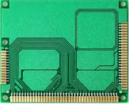
A green solder mask is applied over a white silkscreen legend. This classic combination offers high contrast for component designation markings, aiding in the assembly and debugging processes. The white silkscreen on a green background ensures excellent readability.
Target Applications
This HDI 10-Layer PCB is specifically designed for the consumer electronics HDI PCB board market. Its combination of high layer count, minimal thickness, and fine-line geometry makes it perfect for:
1、Advanced Smartphones and Tablets
2、High-Performance Wearable Technology
3、Compact IoT and Networking Devices
4、Dense Radio Frequency (RF) Modules
The detailed specifications of this HDI 10-Layer Mouse Bite PCB highlight its capability to meet the rigorous demands of next-generation consumer electronics. From its robust SY S1000-2 core and advanced 1+4+1 build-up to its precise 3/3 mil trace/space and reliable ENIG finish, every aspect is tailored for high density, reliability, and performance. Engineers seeking a proven solution for space-constrained, high-speed applications will find this design to be a robust and manufacturable option.
Product Type: High-Density Interconnect (HDI) Printed Circuit Board with Mouse Bite Features
Model Designation: HDI Mouse Bite PCB
Layer Count: 10 Layers
Base Material: SY S1000-2
Stack-up Configuration: 1+4+HDI Build-up
Overall Thickness: 0.8 mm
Copper Weight (Inner/Outer): 1 oz per layer
Solder Mask: Green over White Silkscreen
Surface Finish: Electroless Nickel Immersion Gold (ENIG)
Minimum Trace/Space Width: 3 mil / 3 mil
Target Application: Consumer Electronics HDI PCB Board