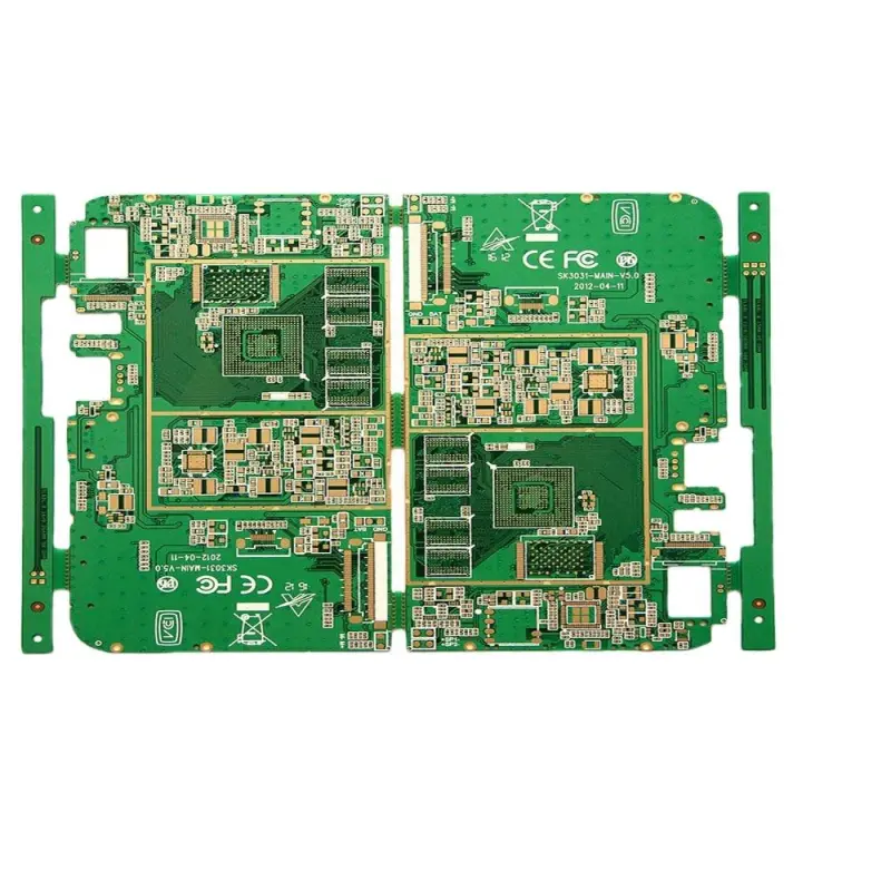
Technical Overview of a 12-Layer HDI PCB for Advanced Smartphone Mainboards
The relentless pursuit of miniaturization and enhanced functionality in smartphones demands highly sophisticated printed circuit board (PCB) technology. This article provides a detailed technical examination of a specialized 12-layer High-Density Interconnect (HDI) PCB engineered specifically for smartphone mainboard applications. The following analysis covers its core specifications, construction, and the manufacturing expertise required to produce such a complex component.
1. Core Material Selection and Board Construction
The foundation of this PCB is a high-performance FR4 laminate, IT180A, with a glass transition temperature (Tg) of 170°C. This high Tg material is selected for its exceptional thermal reliability, mechanical strength, and stability, which are critical for withstanding the thermal stresses of lead-free soldering processes and ensuring long-term device durability.
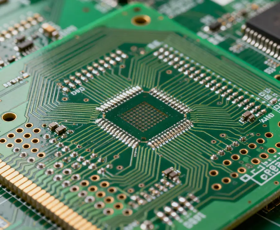
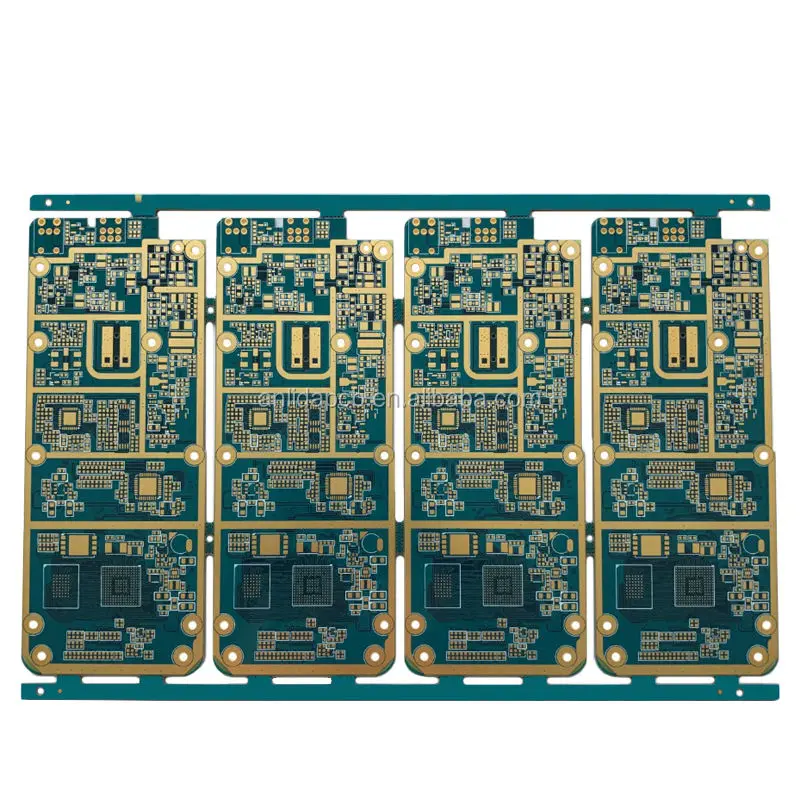
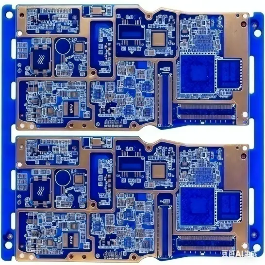
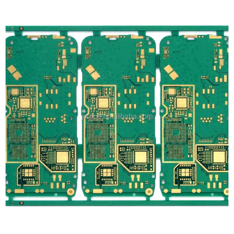
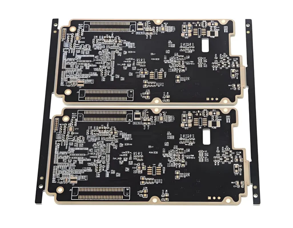
The board features a 12-layer configuration arranged in a 3+6+3 HDI stack-up. This construction signifies a sophisticated build with three sequential HDI layers on both the top and bottom, sandwiching a robust 6-layer core. HDI technology utilizes microvias, blind vias, and buried vias to achieve a higher wiring density per unit area. This is essential for routing the complex circuits of modern processors, memory chips, and RF modules within the confined space of a smartphone. The result is a compact, lightweight, yet highly reliable mainboard.
2. Critical Physical and Electrical Specifications
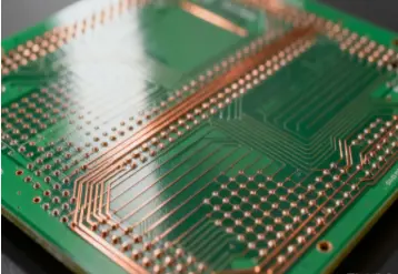
Precision in manufacturing is paramount. The board has a finished thickness of 1.0mm, a standard that offers an optimal balance between structural rigidity and space savings. The copper traces are fabricated with a weight of 0.5 oz, supporting fine-line etching for intricate circuitry.
A key indicator of advanced manufacturing capability is the minimum trace width and spacing, both specified at 2.5 mil (0.0635 mm). Achieving this fine line geometry is necessary for high-speed signal integrity and component density, allowing for more connections in a smaller area.
3. Surface Finish and Solder Mask
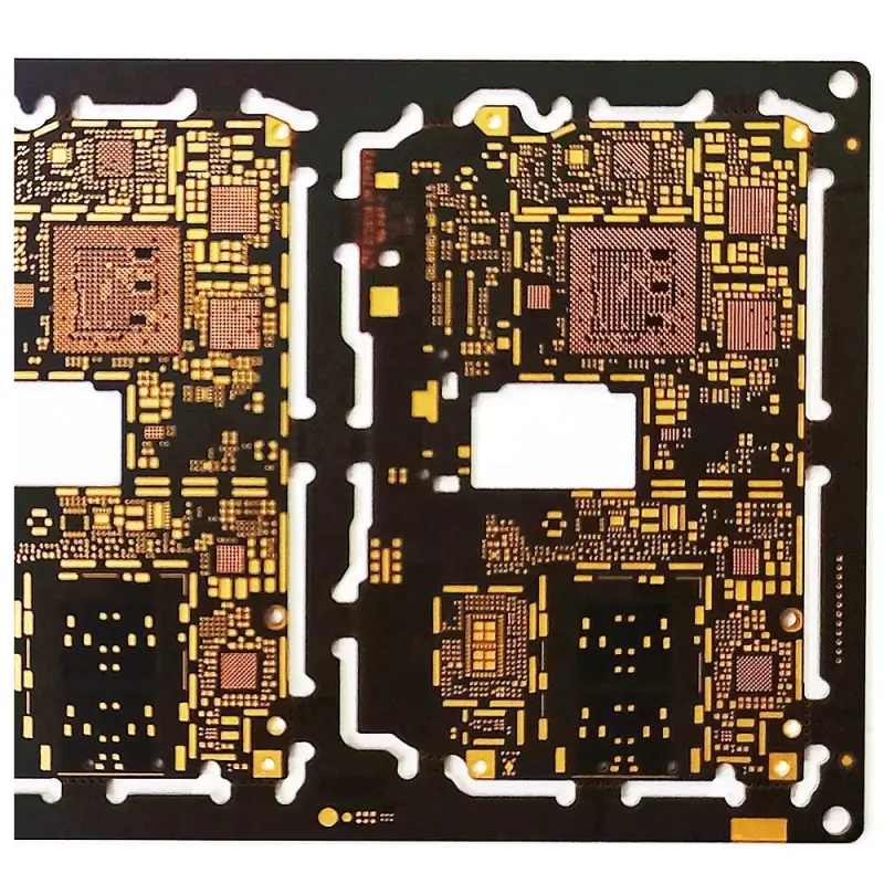
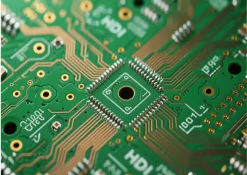
The surface finish is Immersion Gold (ENIG - Electroless Nickel Immersion Gold). This finish provides a flat, uniform surface ideal for the secure soldering of fine-pitch Ball Grid Array (BGA) and chip-scale packages. The nickel layer acts as a diffusion barrier, while the thin gold layer ensures excellent oxidation resistance and shelf life.
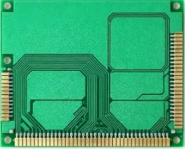
The solder mask is available in both blue and white, serving not only for aesthetics but more importantly for electrical insulation, preventing solder bridges between closely spaced components during assembly.
4. Application and Manufacturing Significance
This PCB is explicitly designed for smartphone mainboard applications. Its 12-layer HDI architecture is tailored to support the high-speed data transmission, power management, and complex signal processing required by today's 5G-capable devices. Manufacturing such a board requires state-of-the-art equipment and stringent process control, particularly in laser drilling for microvias and precise lamination for the multi-layer structure.
The specifications outlined—from the 12-layer 3+6+3 HDI construction to the 2.5 mil trace/space and ENIG finish—represent the high end of PCB technology for the mobile industry. This level of engineering is fundamental to enabling the powerful, compact, and feature-rich smartphones that define the current market. For OEMs and engineers, partnering with a manufacturer capable of consistently producing to these exacting standards is a critical step in product development.
Layer Count: 12 layers
Base Material: IT180A TG170 FR4
Board Construction: 3+6+3 HDI (High-Density Interconnect) structure
Finished Thickness: 1.0 mm
Copper Weight: 0.5 oz
Solder Mask Color: Blue/White
Surface Finish: Immersion Gold (ENIG)
Minimum Trace/Space: 2.5 mil / 2.5 mil
Application: Smartphone mainboard circuitry