Printed Circuit Board")
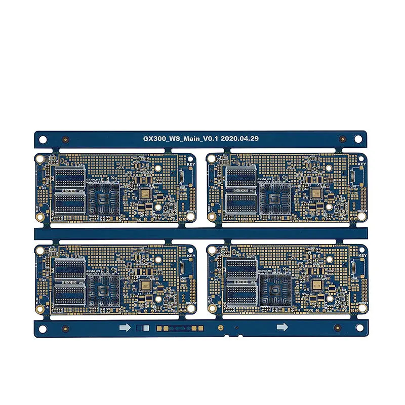
In the landscape of modern electronics, the demand for greater functionality in smaller form factors is relentless. High-Density Interconnect (HDI) Printed Circuit Boards (PCBs) are the engineered solution to this challenge, enabling superior performance and miniaturization. As a specialist HDI PCB manufacturer, we provide the advanced capabilities needed to turn complex designs into reliable, high-yield production reality. This outline details our core technical competencies that cater to the most demanding applications in telecommunications, computing, and advanced consumer electronics.
Our manufacturing process is built on a foundation of precision, versatility, and stringent quality control. Below, we break down the key specifications that define our advanced HDI PCB offerings.
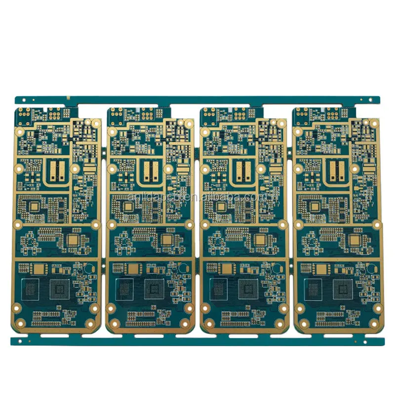
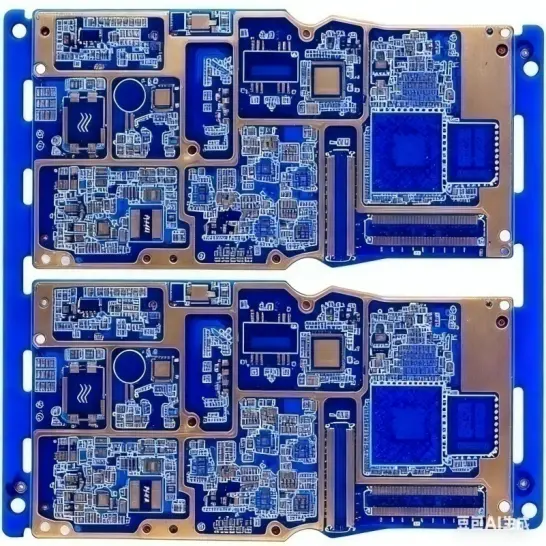
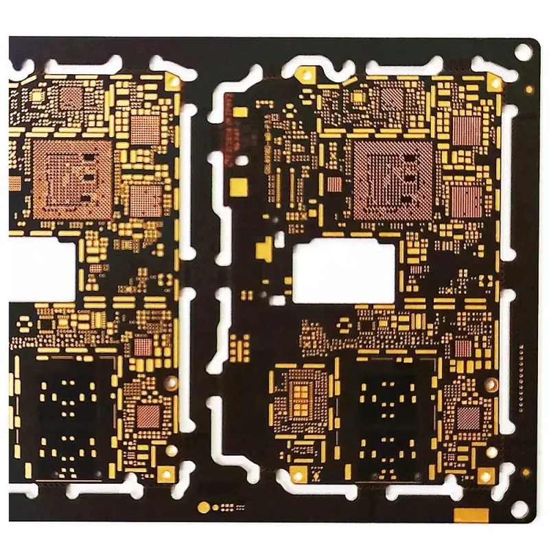
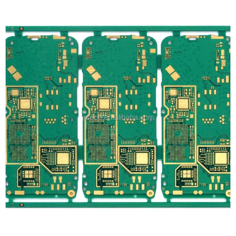
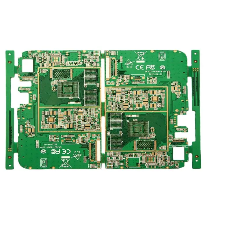
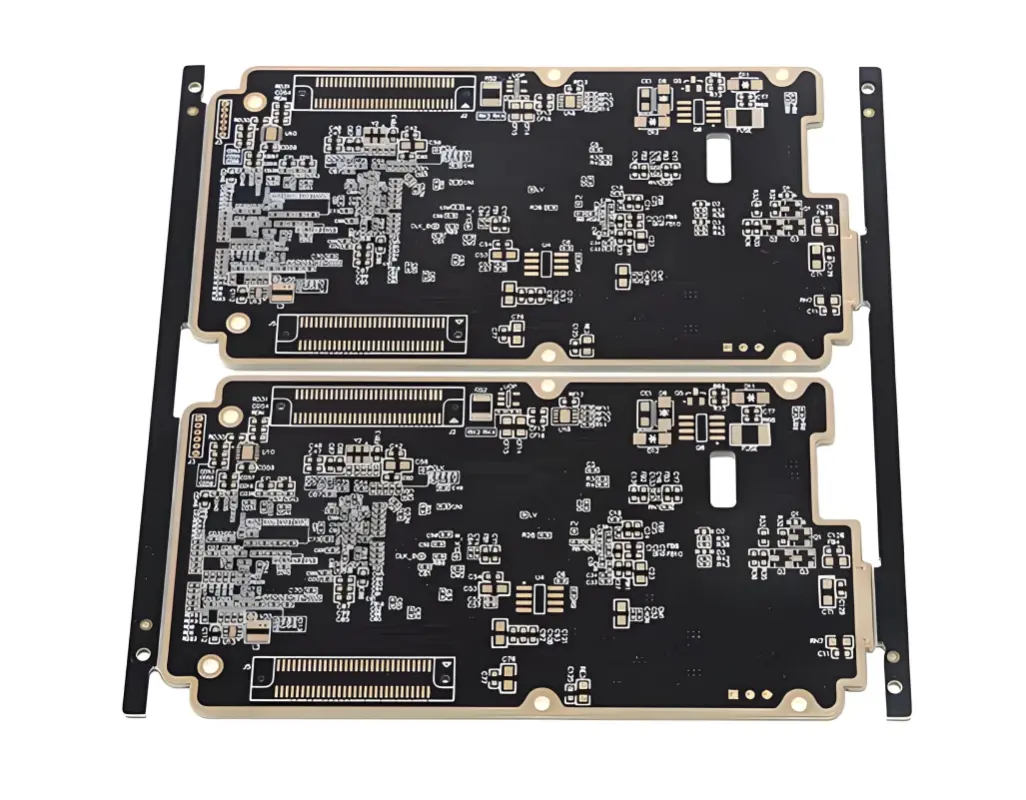
We support a comprehensive range of designs with layer counts extending from 4 to 48 layers. This allows us to accommodate everything from simple, compact devices to highly sophisticated, multi-functional systems. To ensure signal integrity and thermal reliability, we partner with leading laminate suppliers, offering materials from Shengyi, ITEQ, Panasonic, and Tuc. This selection guarantees that each board is built on a foundation optimized for its specific electrical and mechanical requirements.
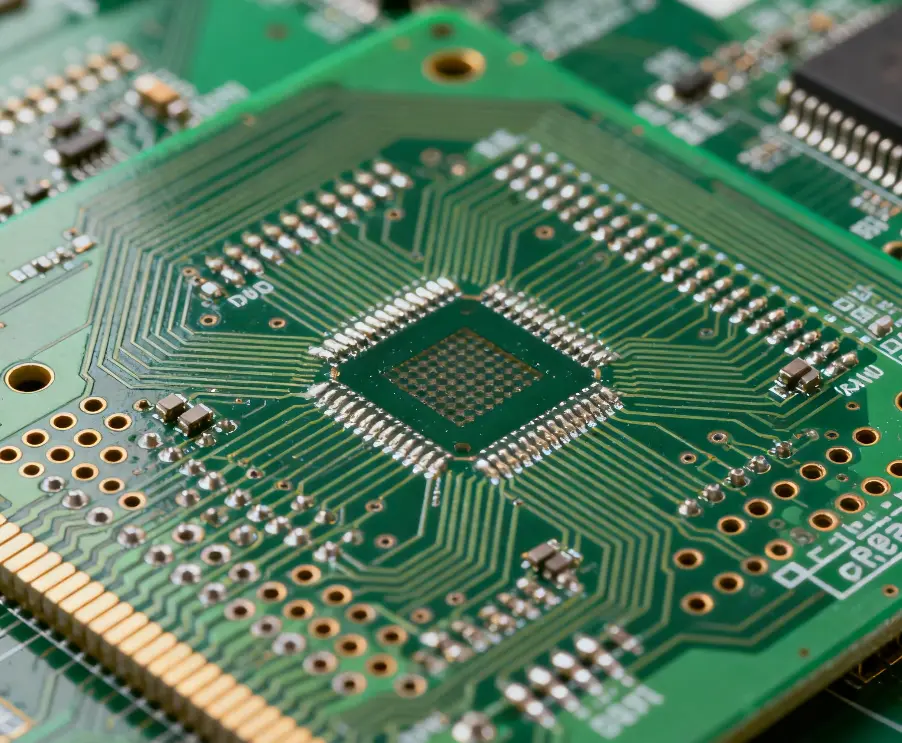
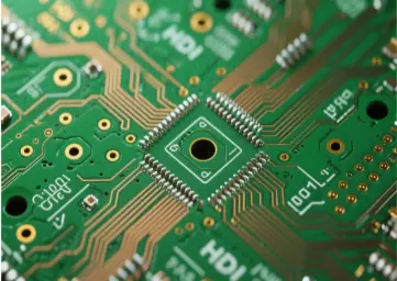
The heart of HDI technology lies in its construction. We excel in both sequential lamination builds (1-5N) and cutting-edge anylayer HDI technology. Anylayer HDI, a significant advancement, allows any layer within the PCB stack-up to be interconnected using laser microvias. This provides maximum design flexibility for routing complex, high-pin-count components like BGAs, effectively reducing board size while enhancing electrical performance.
We maintain precise control over physical board parameters, with a finished thickness range of 0.3 mm to 3.2 mm for both standard and ultra-thin applications. Standard finished copper weights of 0.5 oz and 1.0 oz are offered for optimal current carrying capacity. A critical measure of our advanced fabrication capability is the achievement of 2 mil trace/space routing, particularly in BGA areas, which is essential for interfacing with today's fine-pitch integrated circuits.
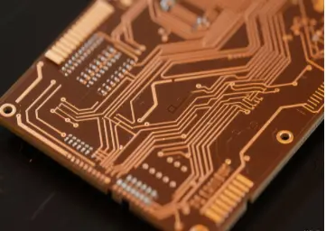
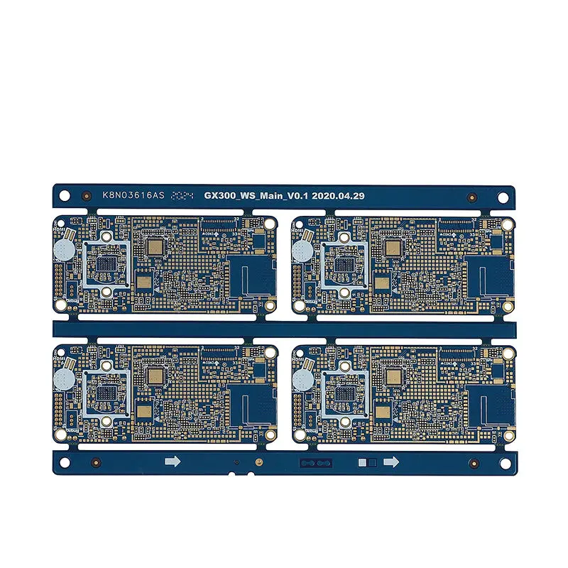
The final surface finish is crucial for assembly yield and long-term reliability. We provide industry-standard options including:
ENIG (Electroless Nickel Immersion Gold): For excellent planarity, solderability, and contact surfaces.
OSP (Organic Solderability Preservative): For a cost-effective, eco-friendly alternative.
Furthermore, we offer specialized control over gold thickness during the ENIG process, a critical factor for applications requiring wire bonding or enhanced corrosion resistance.
Recognizing that aesthetics can serve functional and branding purposes, we provide a standard palette of solder mask colors: Green, White, Black, Red, and Blue.
The specifications detailed above underscore our commitment to supporting innovation at the forefront of electronics. Our capabilities in any-layer HDI, fine-line patterning, and material science are designed to meet the challenges of next-generation products.