Technical Manufacturing Overview: A 12-Layer Any-Layer HDI PCB for Android Mobile Phones
The demand for slimmer, more powerful Android mobile phones drives the need for increasingly sophisticated printed circuit boards (PCBs). The Any-layer High-Density Interconnect (HDI) PCB represents the forefront of this technology, enabling the high component density and complex routing required by modern smartphones. This article provides a technical manufacturing overview of a specific 12-layer Any-layer HDI PCB designed for advanced Android mobile applications.
Core Construction and Material Selection
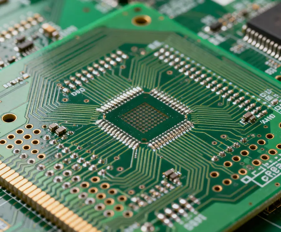
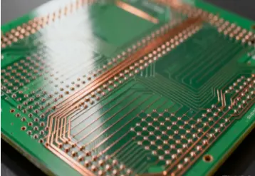
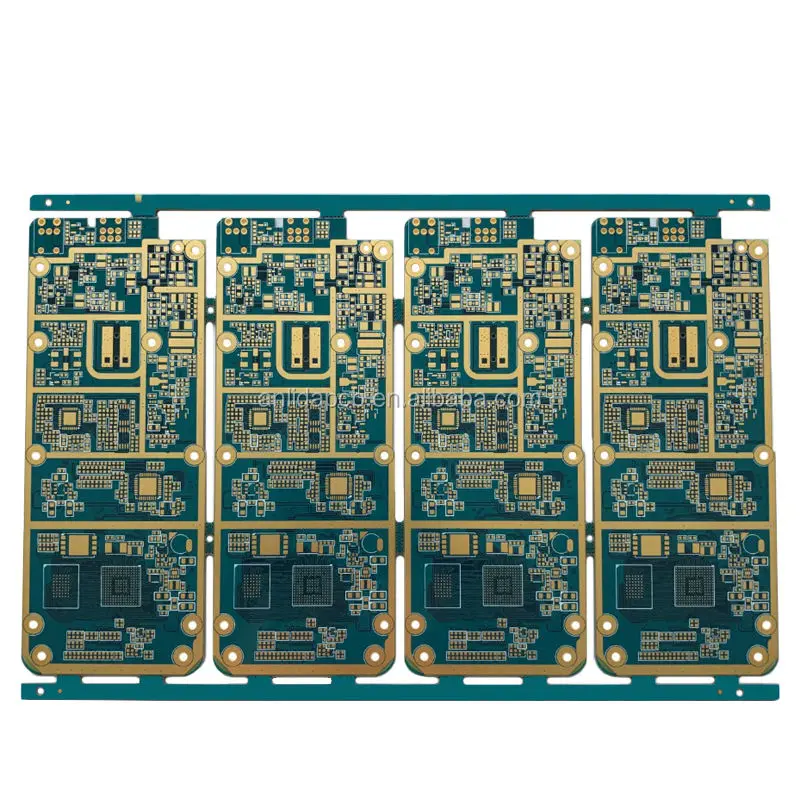
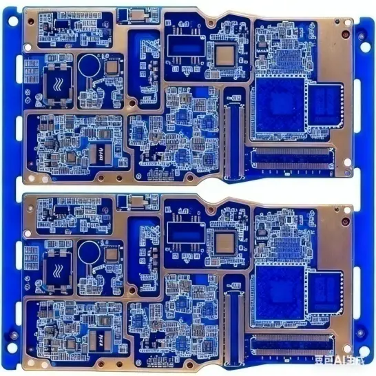
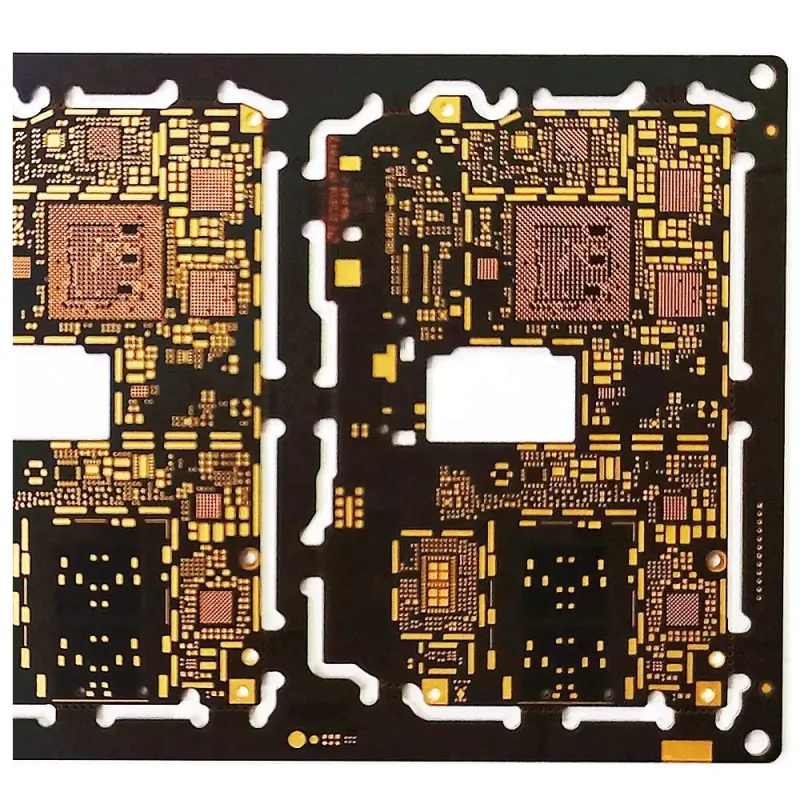
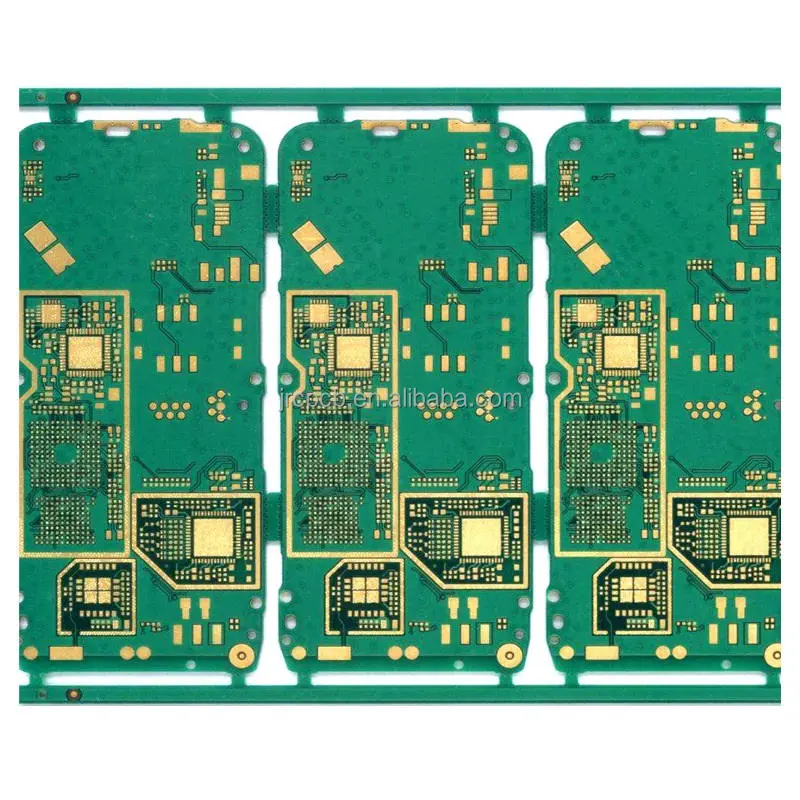
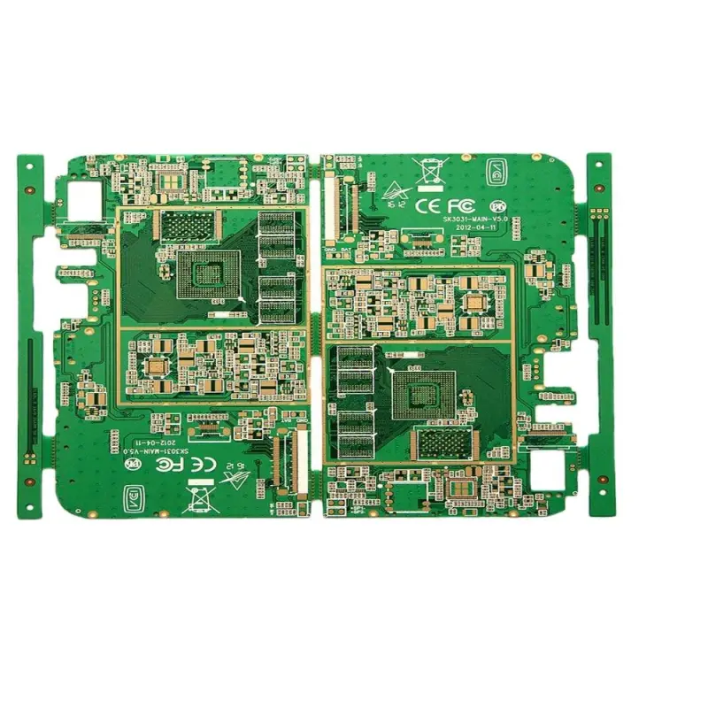
The foundation of this PCB is a 12-layer construction utilizing an Any-layer HDI build-up. Unlike standard HDI which may have defined core layers, the Any-layer process allows microvias to be laser-drilled and stacked on every layer of the board. This provides maximum interconnect density and design flexibility, which is critical for routing the high-pin-count processors and chipsets found in mobile phones.
The base material specified is TUC TU-883, a high-performance, halogen-free laminate and prepreg system. TU-883 is renowned for its excellent thermal reliability, low dielectric loss, and dimensional stability, making it an ideal choice for the thermal stresses of lead-free soldering processes and ensuring stable high-frequency signal integrity.
Critical Manufacturing Specifications
Achieving the target finished board thickness of 1.2mm requires precise control over the lamination of the 12 layers and the dielectric materials. The finished copper weight of 0.5 oz (approx. 17.5 µm) is standard for fine-line circuitry, balancing current-carrying capacity with the need for intricate etching.
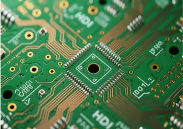
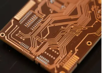
A key indicator of manufacturing precision is the minimum trace width and spacing of 3 mil / 3 mil (75 µm). Producing traces and spaces at this tolerance demands advanced laser direct imaging (LDI) and precise etching processes to ensure uniformity and prevent defects like shorts or opens.
Surface Finish and Solder Mask
The board employs a combination of two surface finishes: Electroless Nickel Immersion Gold (ENIG) and Organic Solderability Preservative (OSP). This hybrid approach allows for optimized performance on different areas of the board. ENIG provides a flat, hard surface ideal for gold wire bonding and fine-pitch components, while OSP protects the copper pads for excellent solderability at a lower cost.
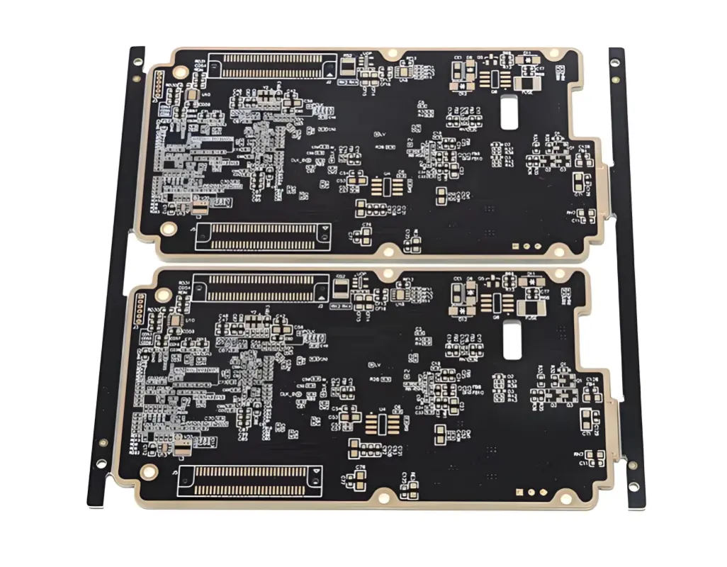
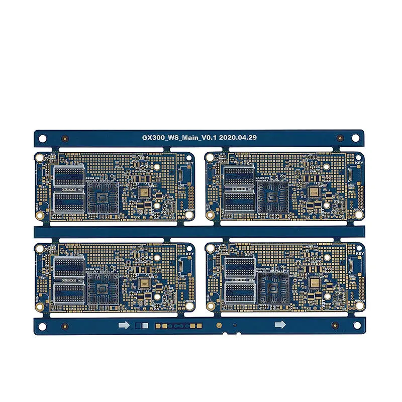
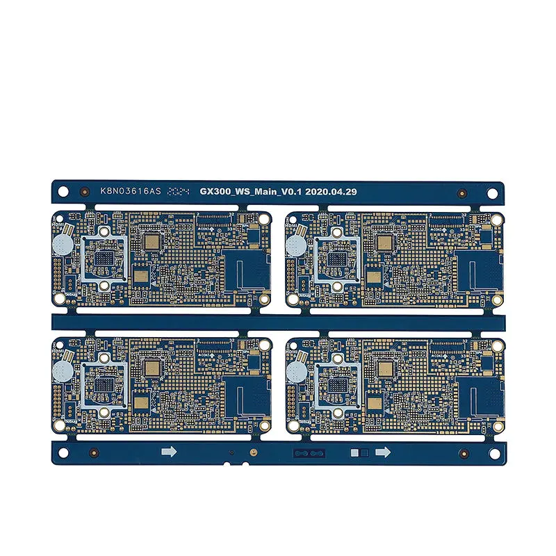
The solder mask is applied in two colors, blue and white, which is common for designating different functional areas or for brand aesthetics within the mobile phone assembly.
Application and Manufacturing Significance
This PCB is explicitly engineered for the Android mobile phone platform. The combination of 12-layer Any-layer HDI construction with high-grade materials and tight tolerances makes it suitable for mid-to-high-tier smartphones where performance, size, and reliability are paramount. The absence of "special technologies" indicates a focus on perfecting core high-density manufacturing processes to ensure yield and reliability.
In summary, this specification sheet outlines the manufacturing blueprint for a high-reliability, high-density PCB. Mastery of materials like TUC TU-883, processes like Any-layer via stacking, and tolerances as tight as 3/3 mil are essential for producing the complex circuits that power today's advanced mobile devices.
Product Category: High-Density Interconnect (HDI) Printed Circuit Board
Application: Android Mobile Phone
Model Designation: Android Mobile Phone Any-layer HDI PCB
Layer Count: 12 Layers
Base Material: TUC TU883
Construction Type: Any-layer HDI Build-up
Final Board Thickness: 1.2 mm
Copper Weight (Finished): 0.5 oz
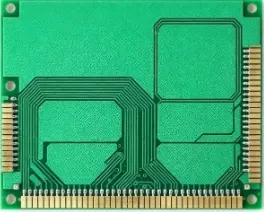
Solder Mask Color: Blue and White
Surface Finish: ENIG (Electroless Nickel Immersion Gold) + OSP (Organic Solderability Preservative)
Special Technologies: None Applied
Minimum Line Width / Spacing: 3 mil / 3 mil