Achieving High-Frequency Performance: Critical Manufacturing Parameters for Microwave PCBs
Microwave Printed Circuit Boards (PCBs) form the backbone of modern high-frequency electronics, enabling applications from radar systems and satellite communications to advanced 5G infrastructure. Unlike standard digital or analog boards, microwave PCBs operate at frequencies where the properties of the substrate and the precision of the manufacturing process directly dictate system performance. Success in this domain hinges on a deep understanding and strict control of a specific set of technical parameters.
This article details the essential manufacturing considerations for engineers designing and specifying PCBs for microwave and RF applications
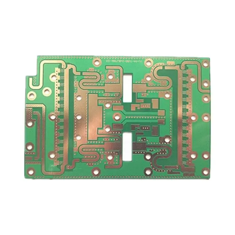
1. Substrate Material: The Foundation of Signal Integrity
The choice of laminate is the most critical decision in microwave PCB design. Standard FR-4 materials are unsuitable due to their high and inconsistent dielectric loss at microwave frequencies.
Low-Loss Laminates: Materials like Rogers RO4000® series, Taconic TLY, and Arlon AD Series are industry standards. They are typically ceramic-filled PTFE composites or hydrocarbon-based ceramics, offering a stable Dielectric Constant (Dk) and an extremely low Dissipation Factor (Df), often below 0.004. This stability is crucial for minimizing signal attenuation and phase distortion.
Thermal Management: For high-power applications, substrates with high Thermal Conductivity (e.g., Rogers TC系列 > 1.0 W/m/K) are essential to dissipate heat effectively and prevent performance drift.
2. Precision Design and Impedance Control
At microwave frequencies, PCB traces function as transmission lines. Any inconsistency becomes a point of signal reflection and loss.
Tight Impedance Tolerance: Achieving and maintaining a precise characteristic impedance (e.g., 50Ω or 75Ω) is paramount. Tolerances must be held to ±5% or tighter (±3% is often targeted). This requires sophisticated modeling of microstrip, stripline, or grounded coplanar waveguide structures.
Strict Dimensional Control: Consistent electrical performance demands exceptional manufacturing precision. Trace width and spacing tolerances are typically controlled to within ±0.02 mm. Similarly, layer-to-layer registration must be held within ±0.05 mm to prevent impedance variations in multilayer boards.
3. Critical Fabrication Processes for Low Loss
Standard PCB fabrication processes must be refined to meet the demands of microwave materials.
Etching Quality: The etching process must produce traces with smooth, well-defined sidewalls. Roughness increases conductor loss and can impact impedance. Controlled undercut during etching is vital to achieve the designed trace geometry.
Plated Through-Hole (PTH) Quality: Via holes must exhibit excellent plating uniformity to ensure reliable interconnects and consistent grounding. The process must guarantee a robust copper deposit in holes with higher aspect ratios, avoiding voids or thin spots that could fail under thermal stress.
4. Surface Finish Selection
The final surface finish must protect the copper while ensuring minimal signal loss and reliable solderability for components.
Electroless Nickel Immersion Gold (ENIG) is a widely used, reliable finish. However, note that the nickel layer can introduce some loss at very high frequencies due to its magnetic properties.
Immersion Silver (ImAg) or Electroless Nickel Electroless Palladium Immersion Gold (ENEPIG) are excellent alternatives for critical applications where minimal loss is a priority. Bare copper with an Organic Solderability Preservative (OSP) is also an option, though it offers less protection before assembly.
5. Validation and Testing
Verification is not an afterthought but an integral part of the microwave PCB manufacturing flow.
Electrical Testing: Beyond continuity testing, RF structures may require specific testing.
Impedance Testing: Time Domain Reflectometry (TDR) is used to verify impedance profiles across the board.
RF Performance: For prototype runs, it may be necessary to perform insertion loss and return loss measurements on coupon test structures to validate that the fabricated board meets the simulated performance targets.
Manufacturing a high-performance microwave PCB is a collaborative effort between the design engineer and the fabricator. It requires a deliberate selection of specialized materials and a manufacturing process geared toward extreme precision and consistency, not just connectivity. By specifying and controlling these critical parameters—from the substrate's Dk/Df to the final impedance validation—teams can ensure their RF systems deliver the required performance and reliability in the most demanding environments. Partnering with a fabricator who has proven expertise in these areas is essential for first-pass success.
Microwave PCB Manufacturing Technical Parameters
1、Core Materials
Substrate Type: PTFE-based high-frequency materials (e.g., Rogers series), Ceramic-filled PTFE composites, Hydrocarbon-based (HBN) laminates
Dielectric constant: 2.2 to 10.0+ (selected based on design), Tolerance tightly controlled to ±0.05 or better
Tangent of the loss angle: Very low, typically in the range of 0.0009 (e.g., RT/duroid 5880) to 0.004
Thermal conductivity: High thermal conductivity required for some applications (e.g., Rogers TC series, >1.0 W/m/K)
2、Design & Structure
Impedance Control: Tightly controlled, typically ±5% or tighter (e.g., ±3%), modeled for microstrip, stripline, etc.
Trace Width/Space Tolerance: Very tight, typically ±0.02mm or better, to ensure consistent electrical performance
Lamination Registration Tolerance: Tightly controlled within ±0.05mm to prevent misalignment in multilayer boards
Surface Finish: Electroless Nickel Immersion Gold (ENIG), ENEPIG, Immersion Silver, OSP
3、Critical Manufacturing Processes
Hole Plating: High requirements for hole wall quality, using plating processes for high aspect ratios to ensure signal integrity at microwave frequencies
Pattern Etching: Tight control of undercut to ensure smooth trace edges and clean profiles, minimizing signal loss
Lamination Process: Precise control of pressure, temperature, and time to avoid material deformation and changes in dielectric properties
4、RF Performance
Insertion Loss: Required to be very low at target frequencies (e.g., 10GHz, 20GHz)
Phase Consistency: Phase difference between different paths in multi-channel systems must be tightly controlled
Quality Factor (Q-value): Required for circuits like resonators, demanding high-Q materials