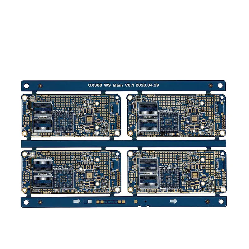
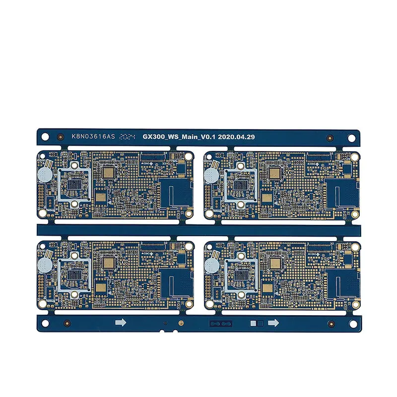
Technical Specifications of an 8-Layer HDI PCB for High-Speed Optical Modules
The demand for higher data rates and greater bandwidth in telecommunications and data centers has pushed the boundaries of printed circuit board (PCB) technology. High-Density Interconnect (HDI) PCBs are at the forefront of this evolution, enabling the sophisticated electronics required for modern optical communication modules. This article details the key manufacturing specifications and technical parameters of an advanced 8-layer PCB engineered specifically for these demanding applications.
Core Construction and Material Selection
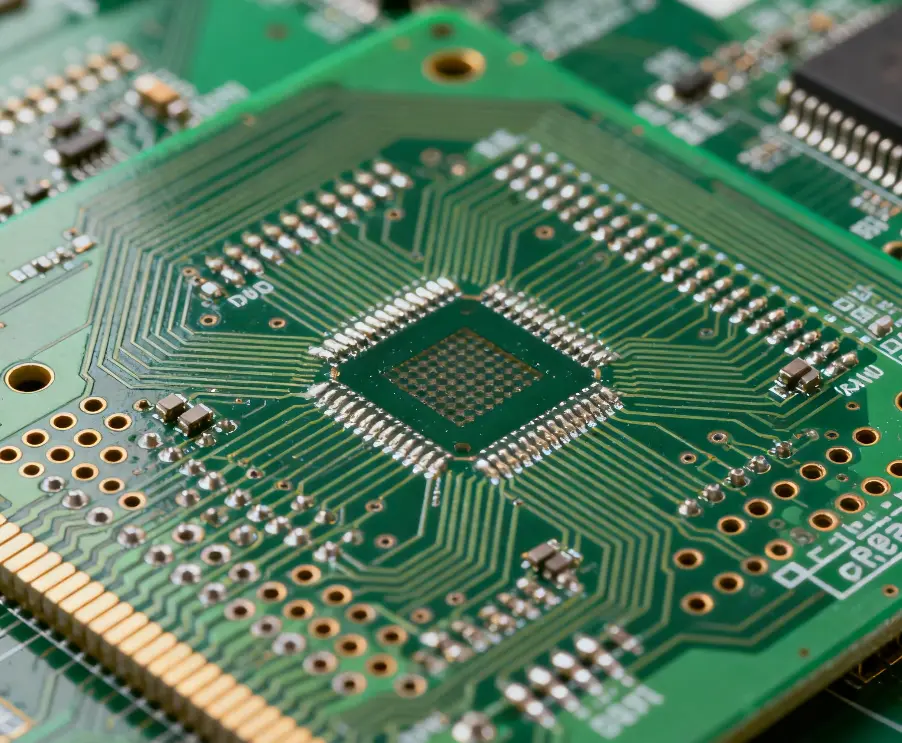
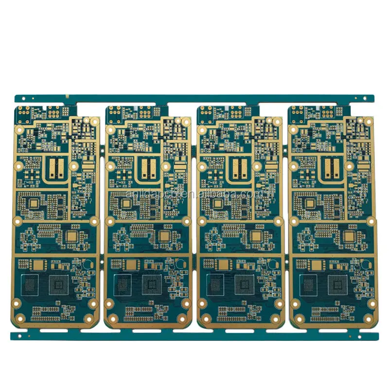
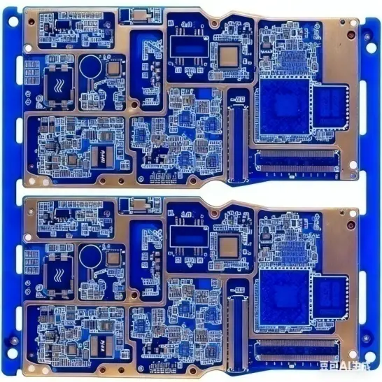
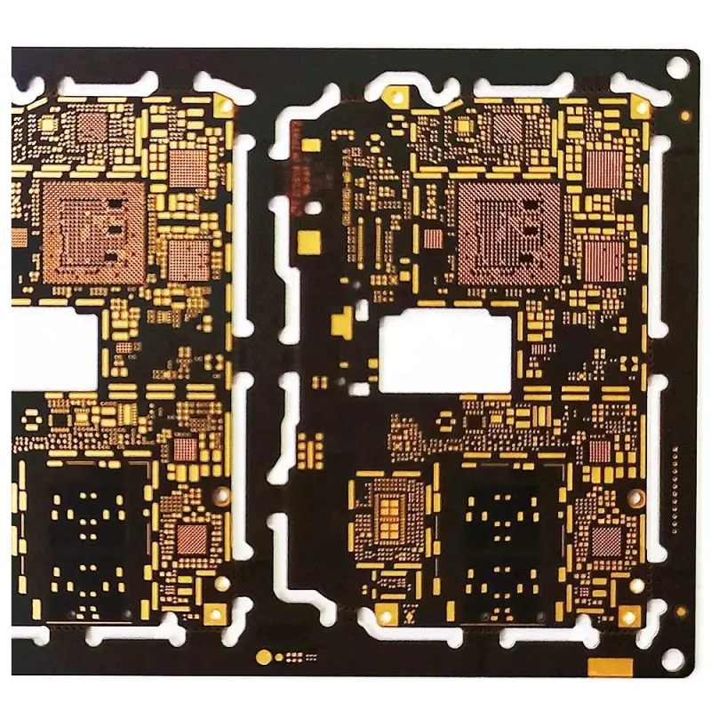
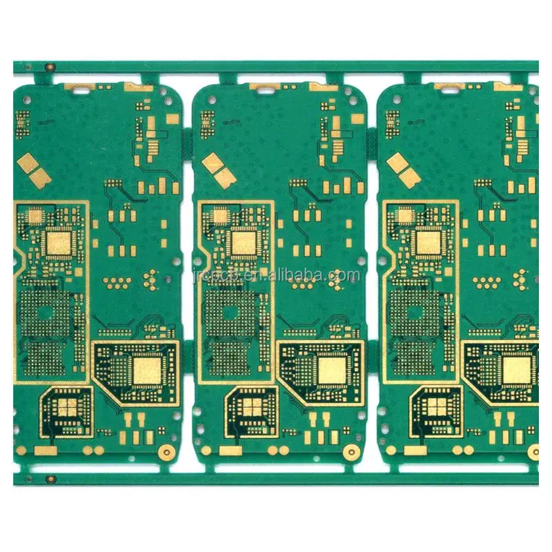
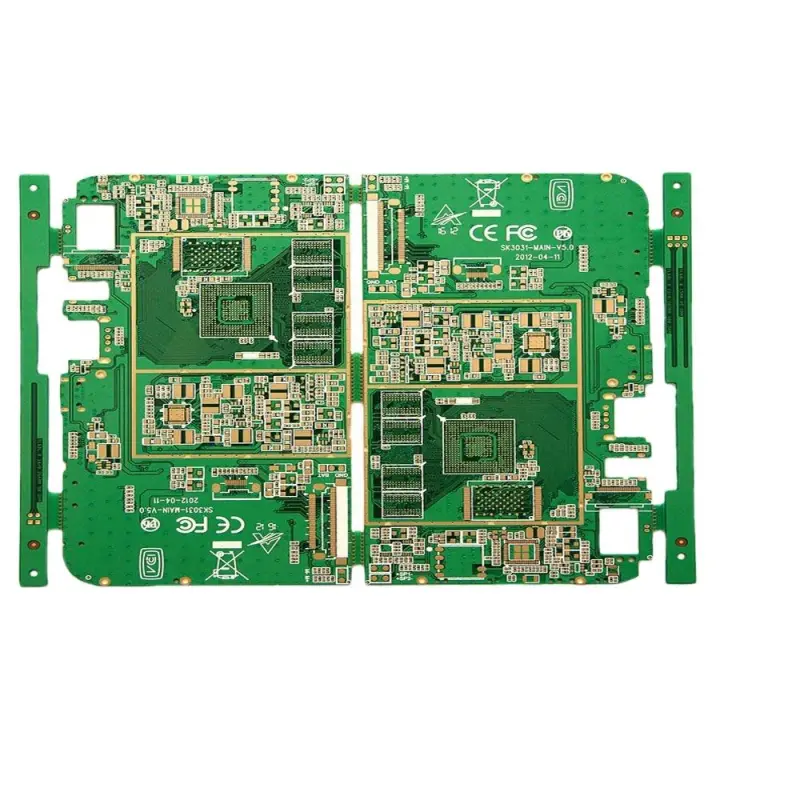
The foundation of this board is a robust 8-layer stack-up with a 2+4+2 HDI construction. This specific buildup indicates the use of microvias and sequential lamination processes, which allow for a higher routing density in a compact form factor. The base material specified is FR-4 with a high glass transition temperature (Tg) of 170°C. The Tg170 rating is critical for optical modules, which often operate in environments with elevated temperatures. This material ensures excellent thermal stability, preventing deformation and maintaining electrical integrity during operation and soldering processes.
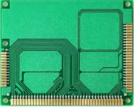
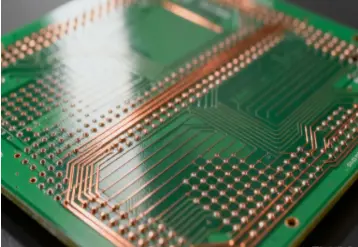
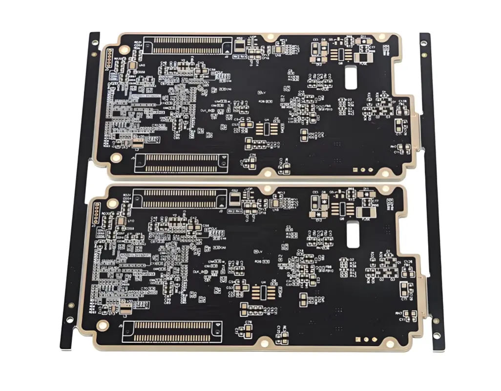
A primary mechanical characteristic is the finished board thickness of 0.8 mm. This slim profile is essential for fitting into the standardized, compact housings of pluggable optical transceivers (e.g., SFP, QSFP). The 1 oz (0.5 oz finished) copper thickness provides a balance between carrying sufficient current and facilitating the precise etching required for ultra-fine features.
Critical Signal Integrity and Surface Finishes
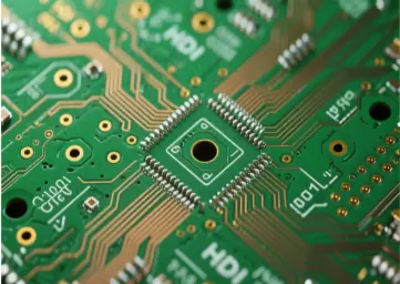
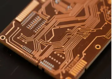
Signal integrity is paramount in high-speed designs. This PCB supports minimum trace width and spacing of 3 mil (approximately 75 microns). This fine-line capability is a hallmark of HDI technology, enabling controlled impedance routing for multi-gigabit serial data signals with minimal loss and crosstalk.
The surface finish is electrolytic hard gold plating. Hard gold, typically a gold-cobalt or gold-nickel alloy, is chosen for its exceptional durability and wear resistance. This is particularly important for the beveled gold fingers (edge connector), which undergo repeated insertion and removal cycles. The beveling of the connector edge ensures smooth mating and prevents damage to the host system's connector socket. The solder mask is available in standard green or white, with white often being preferred for applications where laser marking needs high contrast.
Application and Conclusion
This combination of specifications—8-layer HDI construction with Tg170 material, 3/3 mil trace/space, and a hard gold surface finish—makes this PCB ideal for the core circuitry of optical communication modules. These modules form the backbone of high-speed network infrastructure, including data center interconnects and fiber optic telecommunication systems.
In summary, this set of specifications defines a high-performance, reliable PCB solution tailored for the thermal, mechanical, and electrical challenges of next-generation optical transceivers. Engineers can rely on this design for applications requiring high density, excellent signal integrity, and long-term operational reliability.
Product Model: Optical Module HDI PCB
Layer Count: 8-Layer Stack-up
Base Material: FR-4, Tg170
Board Construction: 2+4+2 HDI (High-Density Interconnect) Buildup
Final Board Thickness: 0.8 mm
Finished Copper Weight: 0.5 oz
Solder Mask Color: Green / White
Surface Finish: Electrolytic Hard Gold Plating
Special Feature: Beveled Gold Fingers (Edge Connector)
Minimum Trace / Space: 3 mil / 3 mil
Primary Application: Optical Communication Module