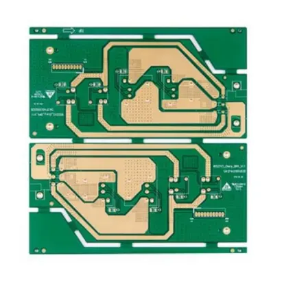
In the rapidly evolving electronics industry, the ability to quickly prototype and manufacture high-quality printed circuit boards (PCBs) is a critical competitive advantage. Our specialized multilayer PCB fabrication service is engineered to meet this demand, offering a combination of speed, precision, and versatility for a wide range of electronic products. This article details the core technical capabilities that define our rapid-turn manufacturing process.
Our primary focus is on providing expedited, or "quick‑turn," fabrication for complex multilayer board assemblies. This service is designed to accelerate product development cycles—from prototyping to initial production runs—without compromising on quality or reliability.
The following specifications outline the breadth of our manufacturing capacity, ensuring we can meet the stringent requirements of modern electronic design.
Material Selection:
We utilize a diverse range of high‑performance substrates to suit various application needs. Our standard offerings include:
FR‑4: The industry‑standard flame‑retardant laminate for most applications.
Polyimide (PI): Ideal for flexible or rigid‑flex PCBs and high‑temperature environments.
Ceramic: Offers excellent thermal conductivity for high‑power and LED modules.
PTFE (Teflon): The preferred material for high‑frequency RF and microwave circuits.
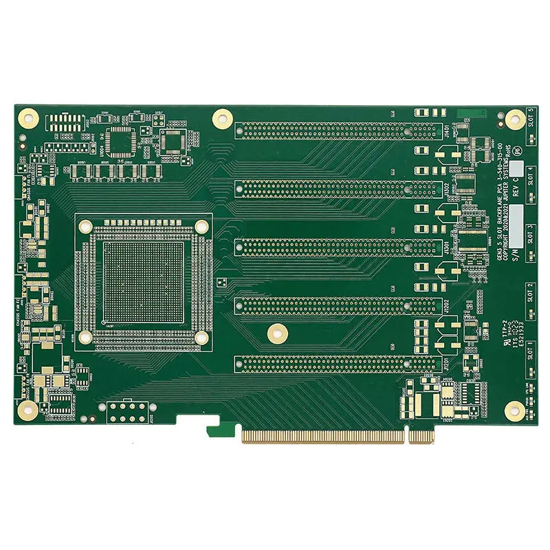
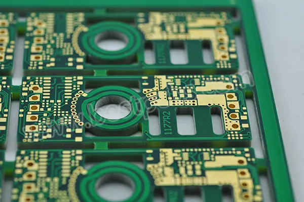
Layer Count Configuration:
We support designs of all complexities, from simple 2‑layer boards to advanced, high‑density multilayer PCBs with intricate interconnect requirements.
Expedited Lead Times:
Speed is a cornerstone of our service. We offer one of the fastest turnaround times in the industry, with standard speedy circuits delivery options as fast as 12 hours from design approval.
Solder Mask Options:
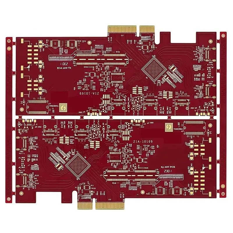
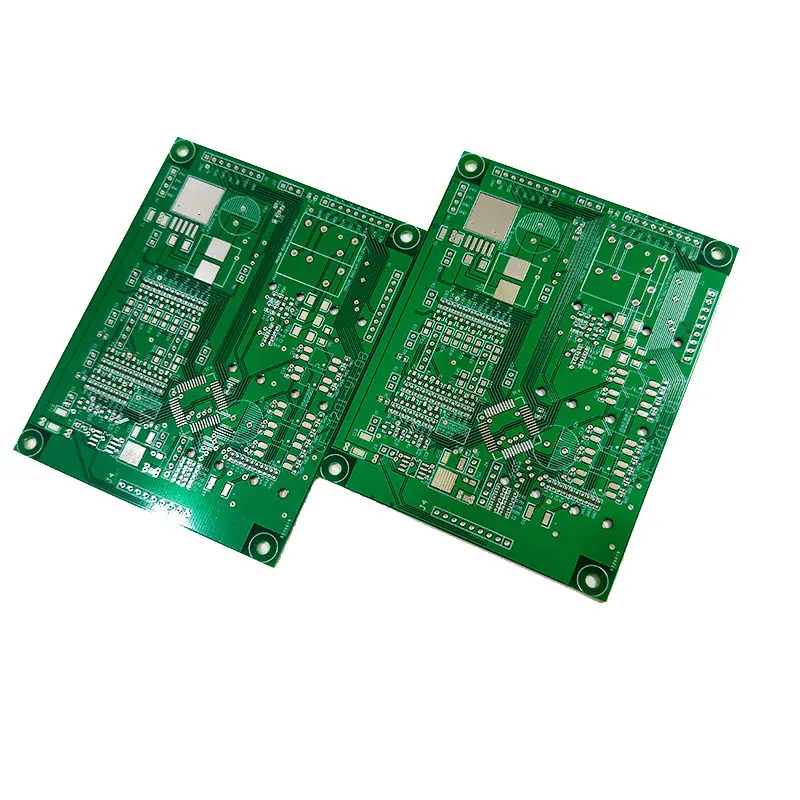
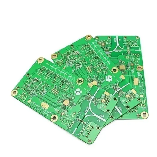
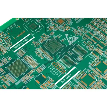
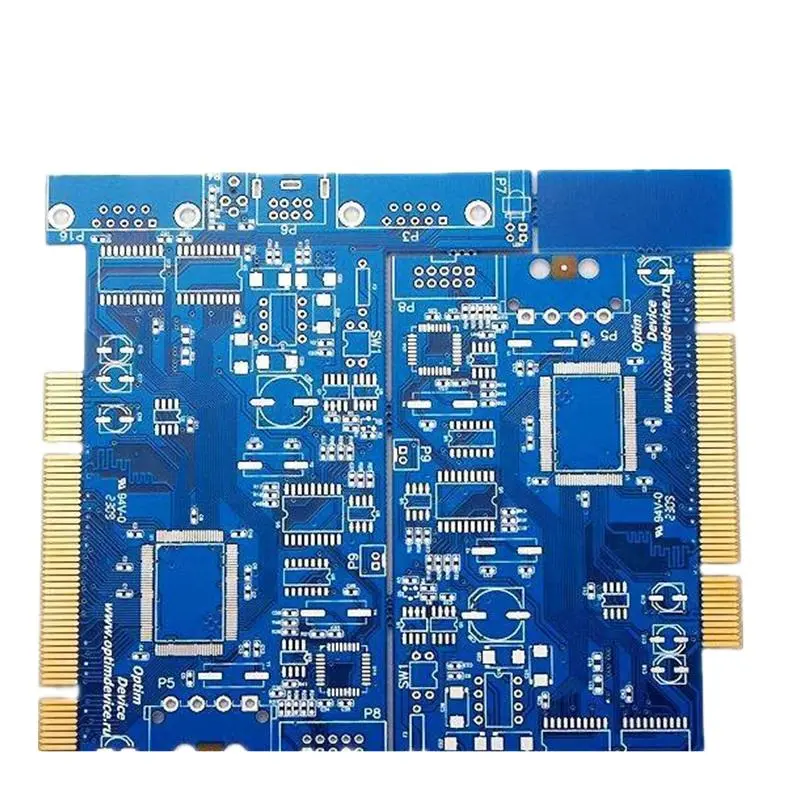
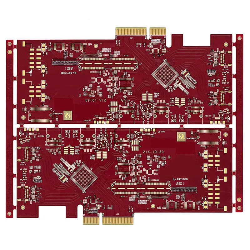
Boards are available in a variety of standard colors to suit aesthetic or organizational preferences, including Green, Blue, Yellow, Red, and Black.
Finished Board Thickness:
We provide precise control over the final board thickness, accommodating a wide range from a slender 0.15 mm up to a robust 6.0 mm.
Copper Weight Flexibility:
To handle different current‑carrying capacities, we can fabricate boards with copper weights ranging from 0.5 oz for fine‑precision signals to a heavy 12 oz for high‑power applications.
Surface Finish Treatments:
A selection of surface finishes is available to ensure solderability and protect the copper traces:
ENIG (Electroless Nickel Immersion Gold): Provides a flat, lead‑free surface excellent for fine‑pitch components.
HASL (Hot Air Solder Leveling): A cost‑effective, traditional finish.
OSP (Organic Solderability Preservative): A flat, RoHS‑compliant organic coating.
Precision and Tolerance:
Our advanced manufacturing equipment achieves a high level of precision, supporting a minimum line width and spacing of 0.1 mm / 0.1 mm. This capability is essential for dense, high‑performance designs.
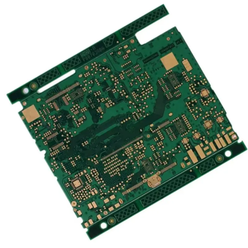
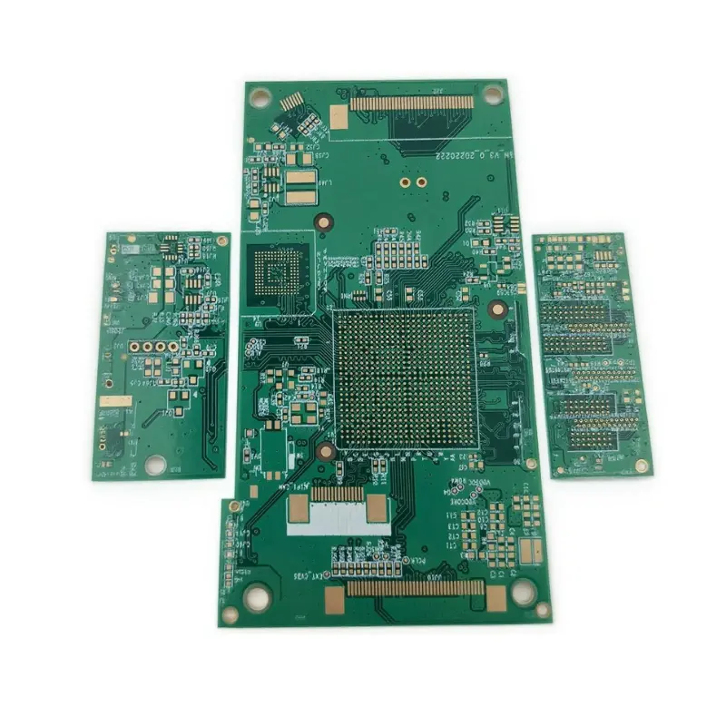
These fabrication capabilities directly support the development of a broad spectrum of electronic products. From consumer gadgets and telecommunications equipment to industrial control systems and medical devices, our rapid‑turn service provides the reliable foundation needed to bring innovative ideas to market faster.
By integrating swift turnaround times with a comprehensive set of technical specifications, our multilayer PCB fabrication service empowers engineers and designers. This commitment to speed, precision, and material versatility ensures that your projects move seamlessly from concept to functional reality, keeping you ahead in a competitive landscape.