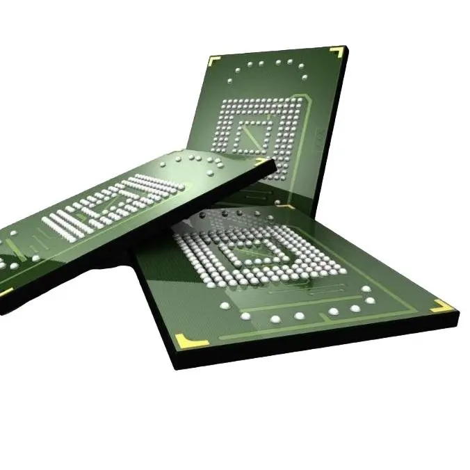
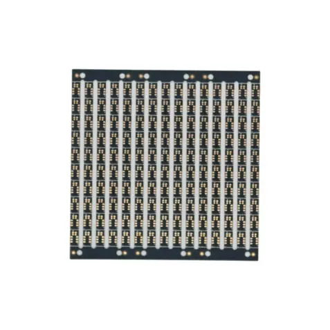
Sensor Integrated Circuit (IC) substrates form the critical interface between sensitive semiconductor dies and the larger system board. This technical data sheet provides a detailed overview of a high‑performance, 4‑layer substrate engineered specifically for demanding sensor applications. Its design emphasizes miniaturization, signal integrity, and reliability under stringent operating conditions.
This substrate is designated for use as a Sensor IC Substrate, indicating its primary role in packaging environments for image sensors, biometric sensors, and other high‑fidelity sensing components where signal accuracy is paramount.
The core construction utilizes Shengyi SI10U, a high‑performance laminate material known for:
Excellent thermal stability
Low dielectric loss
Controlled CTE (Coefficient of Thermal Expansion)
These properties are critical for preventing delamination and maintaining electrical performance during reflow soldering and device operation.
The substrate showcases sophisticated fabrication technology with a minimum trace width and spacing of 35 micrometers (μm) . This fine‑line geometry is essential for achieving the high interconnect density required by modern, multi‑pin sensor ICs.
The surface finish is Electroless Nickel Immersion Gold (ENIG) . This finish provides:
A flat, solderable surface
Excellent oxidation resistance for long shelf life
A reliable contact surface for wire bonding or flip‑chip attachment
Overall Thickness: 0.25 mm —ultra‑thin, supporting the trend towards thinner end products.
Layer Count: 4‑layer construction with specific sub‑composites: 1L‑4L, 1L‑2L, and 3L‑4L.
This complex stack‑up allows for optimized power and signal distribution, shielding critical signals from interference.
Solder Mask: The application of Taiyo PSR‑4000 AUS308 solder mask ensures superior insulation resistance and protection against environmental factors.
Microvia Technology: The substrate incorporates a mixed via architecture:
Laser‑Drilled Microvias: 0.075 mm diameter—enabling high‑density interconnects between layers.
Mechanical Vias: 0.1 mm diameter—used for deeper layer connections.
This combination allows for efficient routing in a compact space.
This Sensor IC Substrate represents a capable solution for advanced semiconductor packaging. The combination of high‑frequency laminate material (SI10U), 35 μm fine‑pitch circuitry, ultra‑thin profile, and ENIG surface finish makes it particularly suited for high‑reliability sensor applications in consumer electronics, automotive, and medical industries. Its specifications meet the rigorous demands for miniaturization and electrical performance in today's competitive market.