PCBA")
 PCBA")
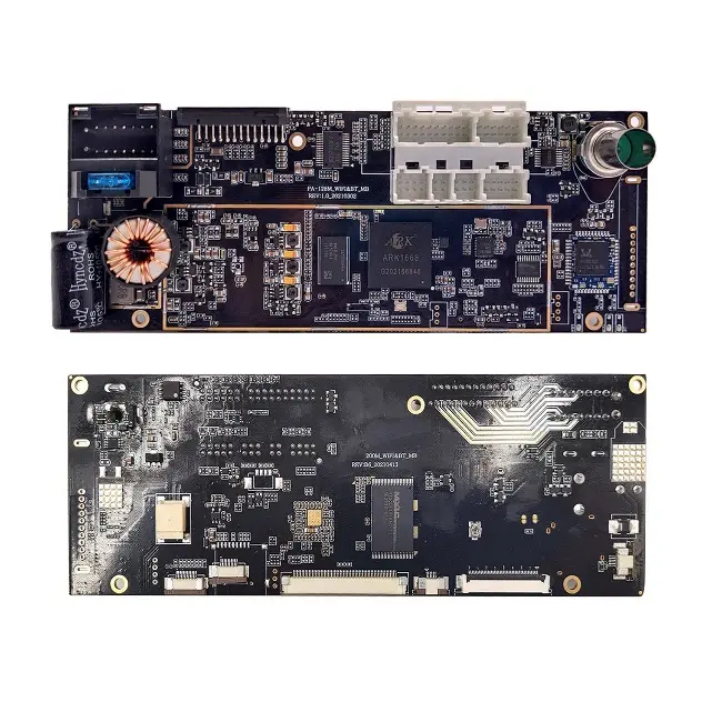
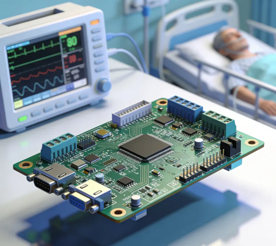
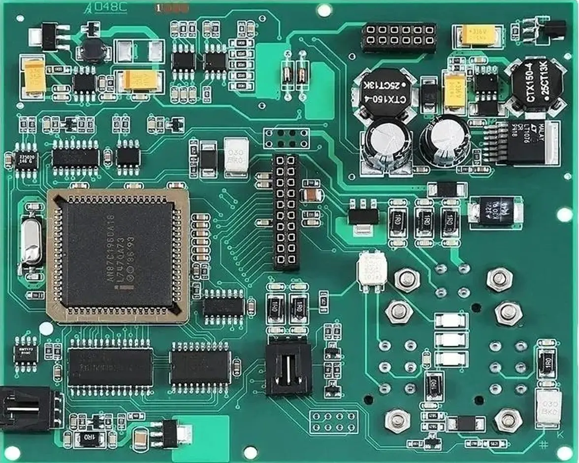
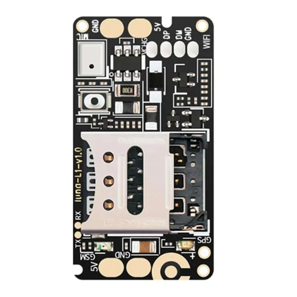
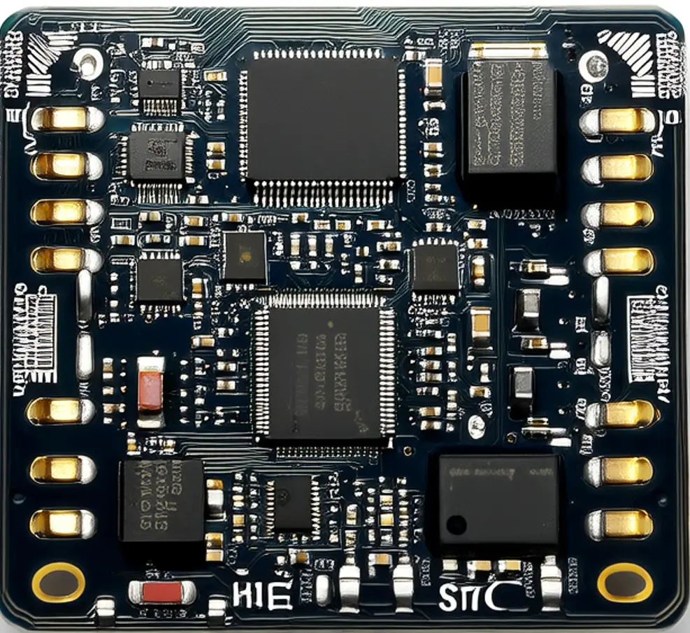
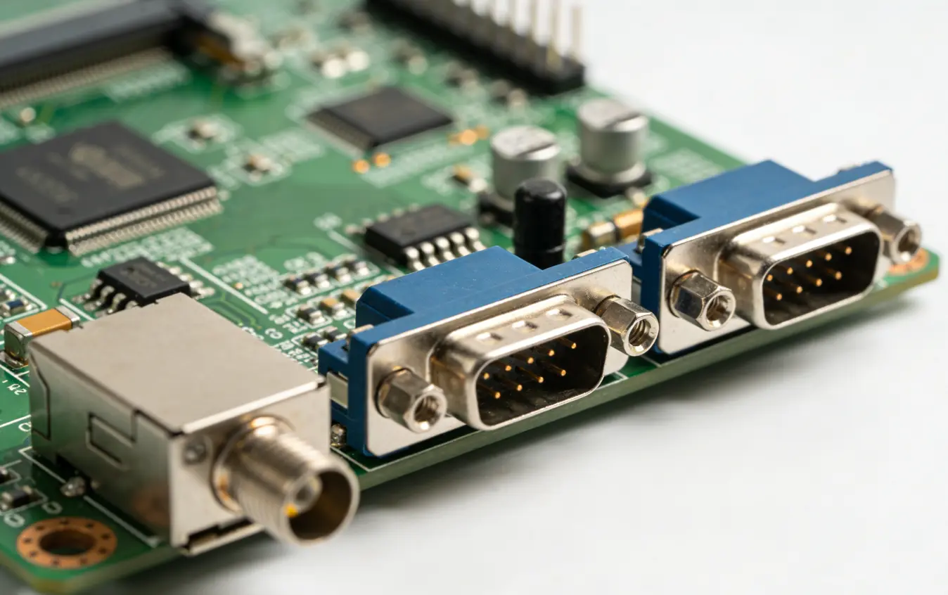
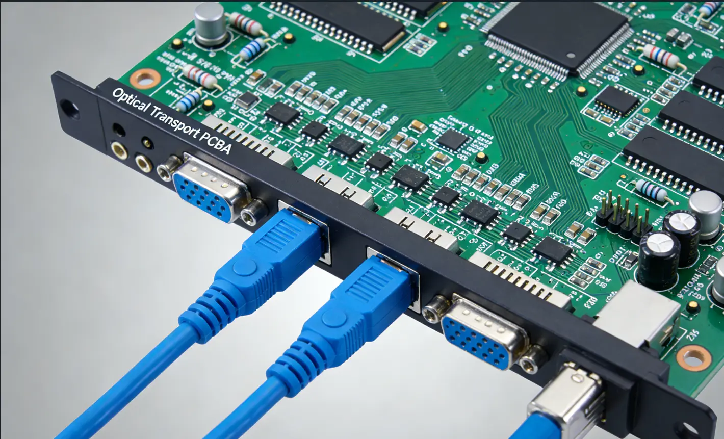
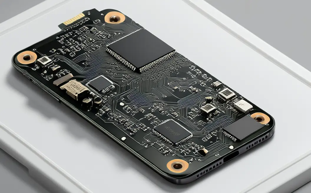
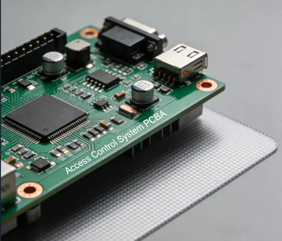
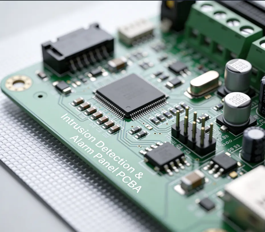
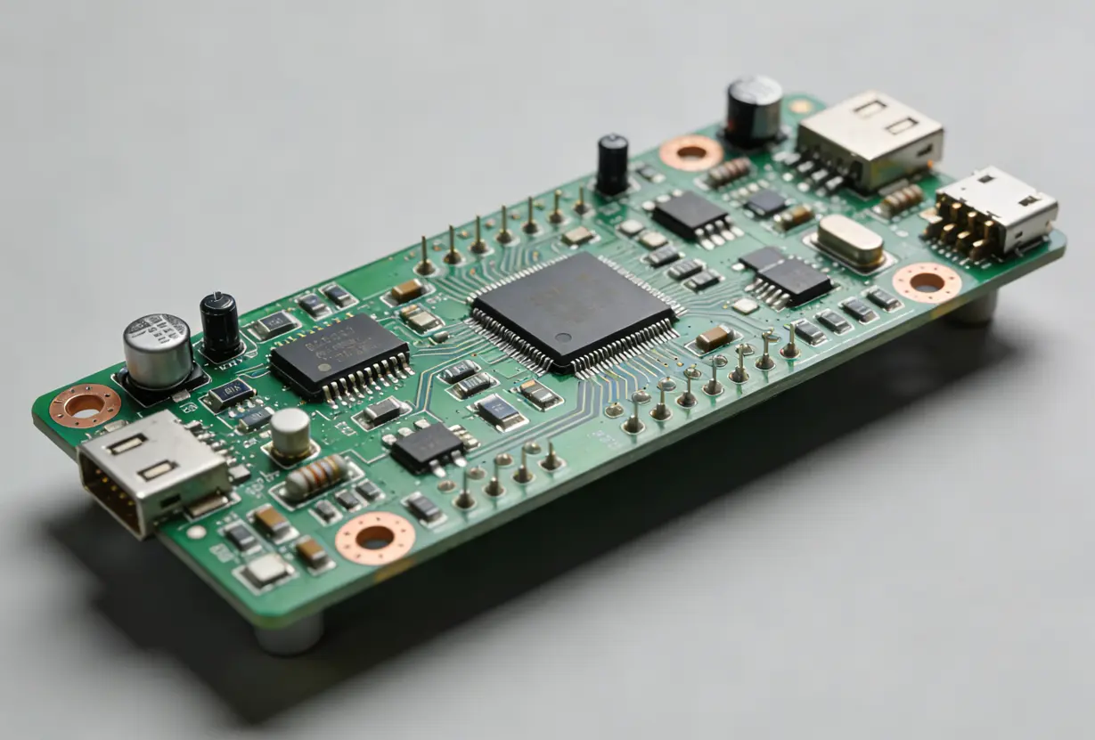
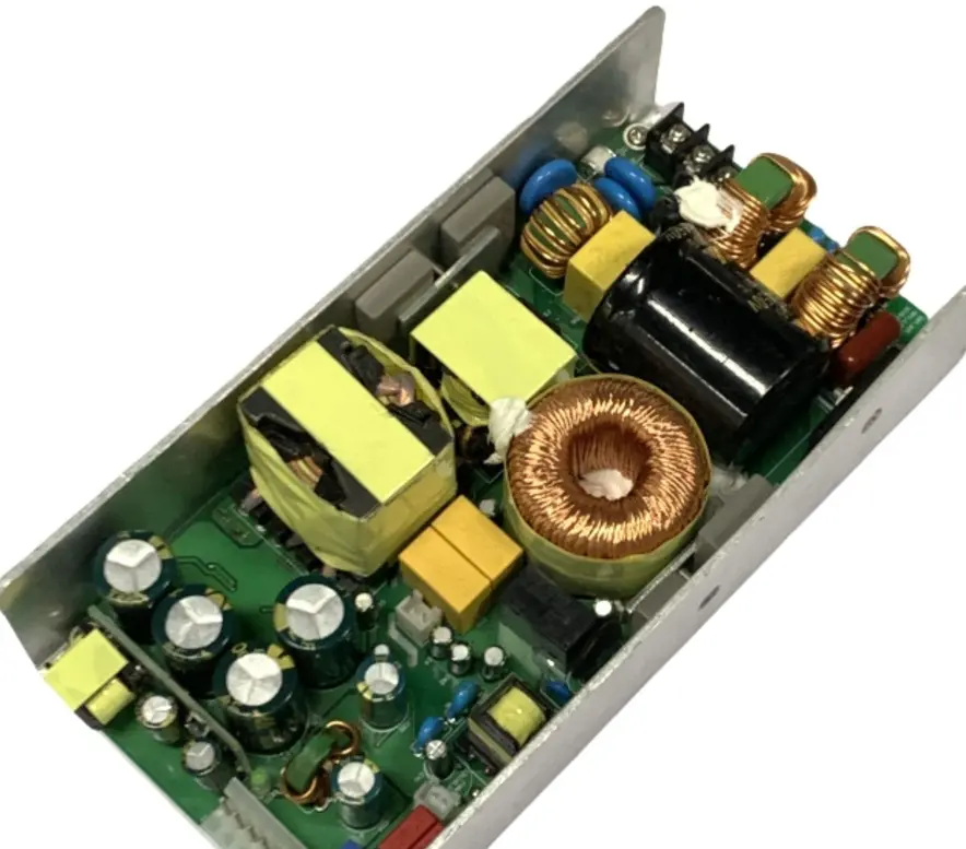
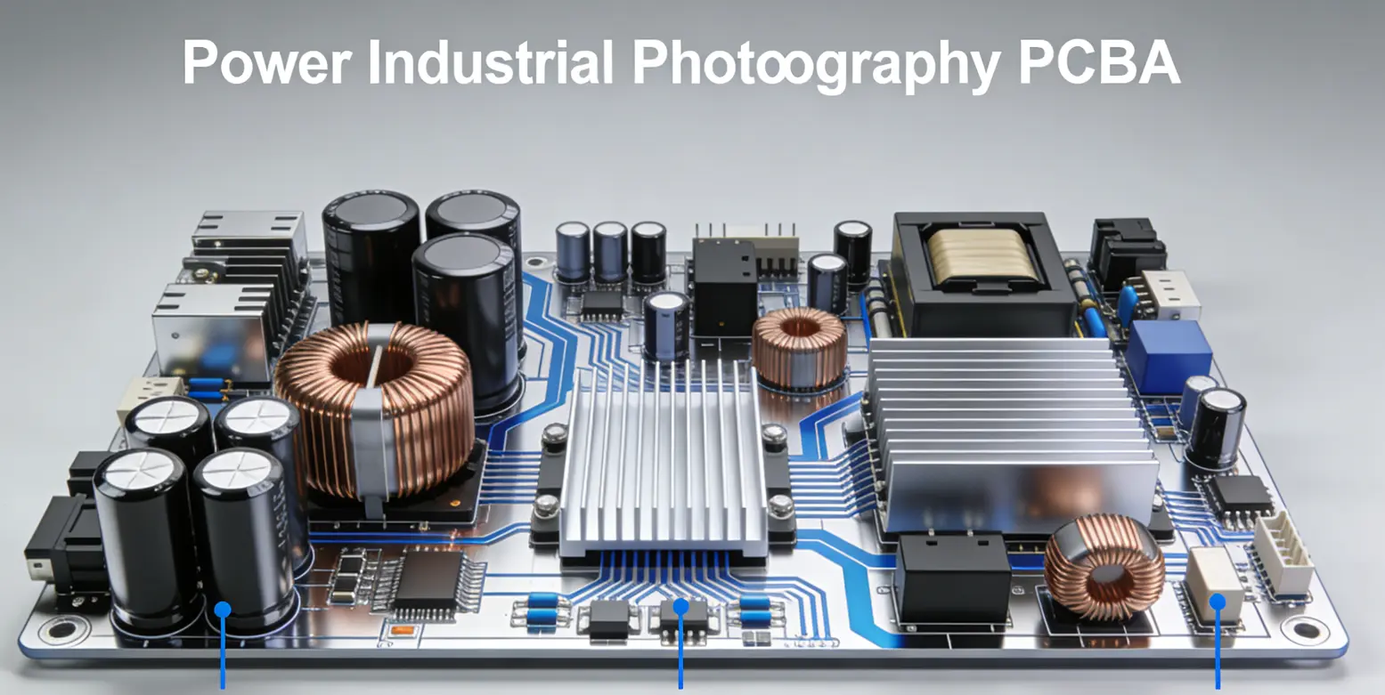
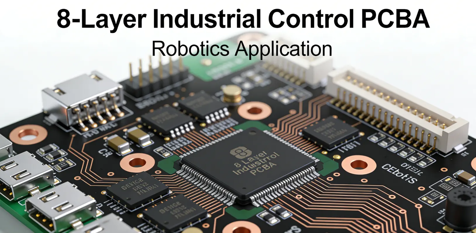
Programmable Logic Controller (PLC) boards are the backbone of modern industrial automation systems. Their reliability directly impacts production uptime, safety, and operational efficiency. As industries push toward greater automation, harsher operating conditions, and longer equipment lifespans, the demand for highly durable PLC boards has never been higher. To meet these demands, manufacturers are increasingly adopting advanced manufacturing methods that go beyond traditional PCB fabrication. This article explores key advanced manufacturing technologies that enhance the mechanical robustness, thermal resilience, electrical integrity, and environmental resistance of PLC boards—ensuring long-term performance in demanding industrial settings.
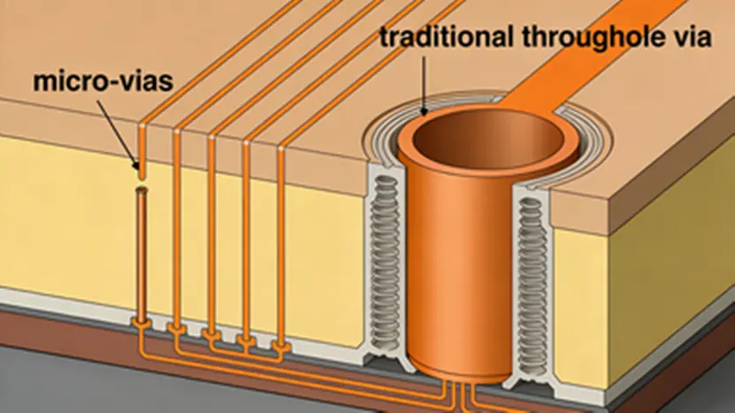
High-Density Interconnect (HDI) technology enables the creation of more compact yet functionally richer PCBs by using microvias, finer traces, and tighter pad spacing. For PLC boards, HDI offers several durability advantages:
· Reduced Layer Count with Enhanced Functionality: Fewer layers mean fewer interlayer interfaces prone to delamination under thermal cycling.
· Improved Signal Integrity: Shorter trace lengths minimize electromagnetic interference (EMI), reducing signal degradation over time.
· Mechanical Stability: Microvia structures (especially stacked or staggered vias) provide stronger interlayer connections compared to traditional through-hole vias, which are susceptible to fatigue in vibration-prone environments.
In industrial applications where PLCs are mounted on moving machinery or exposed to constant mechanical stress, HDI’s structural integrity significantly extends board life.
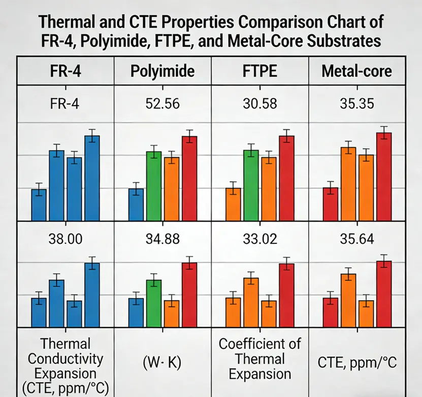
Traditional FR-4 epoxy-glass laminate is cost-effective but lacks the thermal and mechanical performance required for high-reliability PLC applications. Advanced substrate materials offer superior alternatives:
· Polyimide (PI): Known for excellent thermal stability (up to 250°C+), flexibility, and chemical resistance. Ideal for PLCs used in high-temperature environments like steel mills or automotive paint shops.
· PTFE (Teflon): Offers ultra-low dielectric loss and moisture resistance, beneficial in high-frequency communication modules within PLC systems.
· Metal-Core PCBs (MCPCBs): Aluminum or copper cores efficiently dissipate heat from power components (e.g., relays, switching regulators), preventing thermal runaway and solder joint fatigue.
By selecting substrates tailored to specific environmental stresses, manufacturers can dramatically improve PLC board longevity.
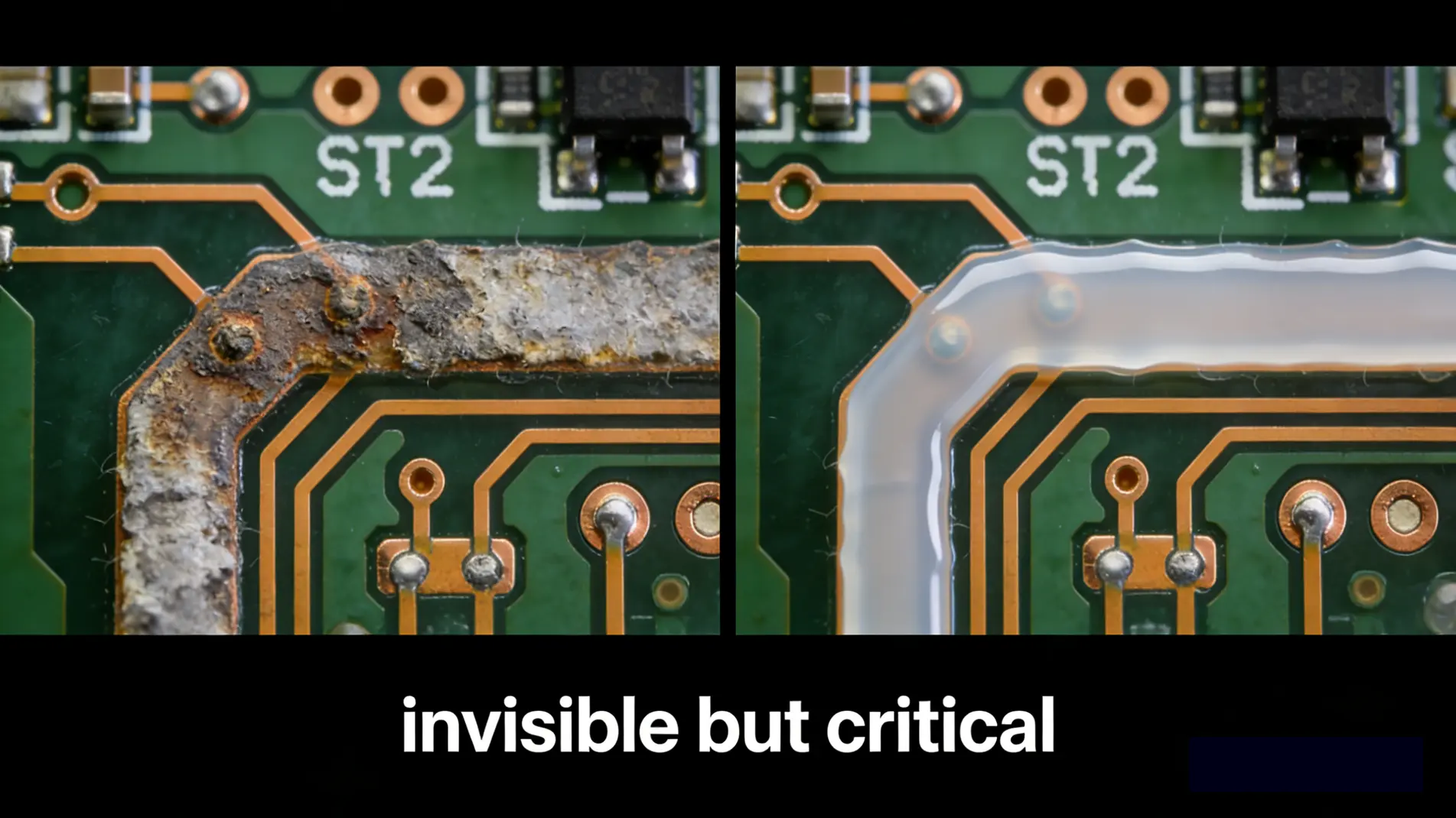
Moisture, dust, chemicals, and salt spray are common threats in industrial facilities. Conformal coatings act as protective barriers applied directly onto assembled PCBs:
· Acrylic Coatings: Easy to apply and repair; suitable for general-purpose protection.
· Silicone Coatings: Flexible and thermally stable; ideal for wide temperature swings.
· Parylene (C or N): Deposited via vapor-phase polymerization, offering pinhole-free, ultra-thin, and chemically inert coverage—even on complex geometries.
For mission-critical PLCs in oil & gas, marine, or food processing plants, parylene coating provides unmatched environmental sealing without adding significant weight or thickness.
Additionally,potting/encapsulation with epoxy or polyurethane resins offers even higher mechanical protection, shock absorption, and complete isolation from contaminants—though at the cost of reparability.
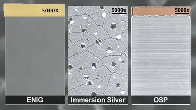
The choice of solder mask and surface finish plays a critical role in long-term corrosion resistance and solder joint reliability:
· ENIG (Electroless Nickel Immersion Gold): Provides a flat, oxidation-resistant surface ideal for fine-pitch components and repeated thermal cycles. Nickel acts as a diffusion barrier, while gold ensures reliable contact.
· Immersion Silver or Tin: Cost-effective alternatives with good solderability, though less durable in sulfur-rich atmospheres.
· OSP (Organic Solderability Preservative): Environmentally friendly but less robust for long-term storage or harsh conditions.
Moreover,selective solder masking—where solder mask is precisely applied only where needed—enhances adhesion in high-vibration zones and prevents tin whisker growth in lead-free assemblies.
Embedding resistors, capacitors, or even ICs within the PCB substrate reduces reliance on surface-mounted parts vulnerable to mechanical shock and thermal stress. Benefits include:
· Lower Profile: Reduces risk of component detachment during impact or vibration.
· Improved EMI Shielding: Internal placement minimizes loop areas and radiated emissions.
· Enhanced Thermal Management: Heat-generating components can be embedded near thermal vias or metal cores.
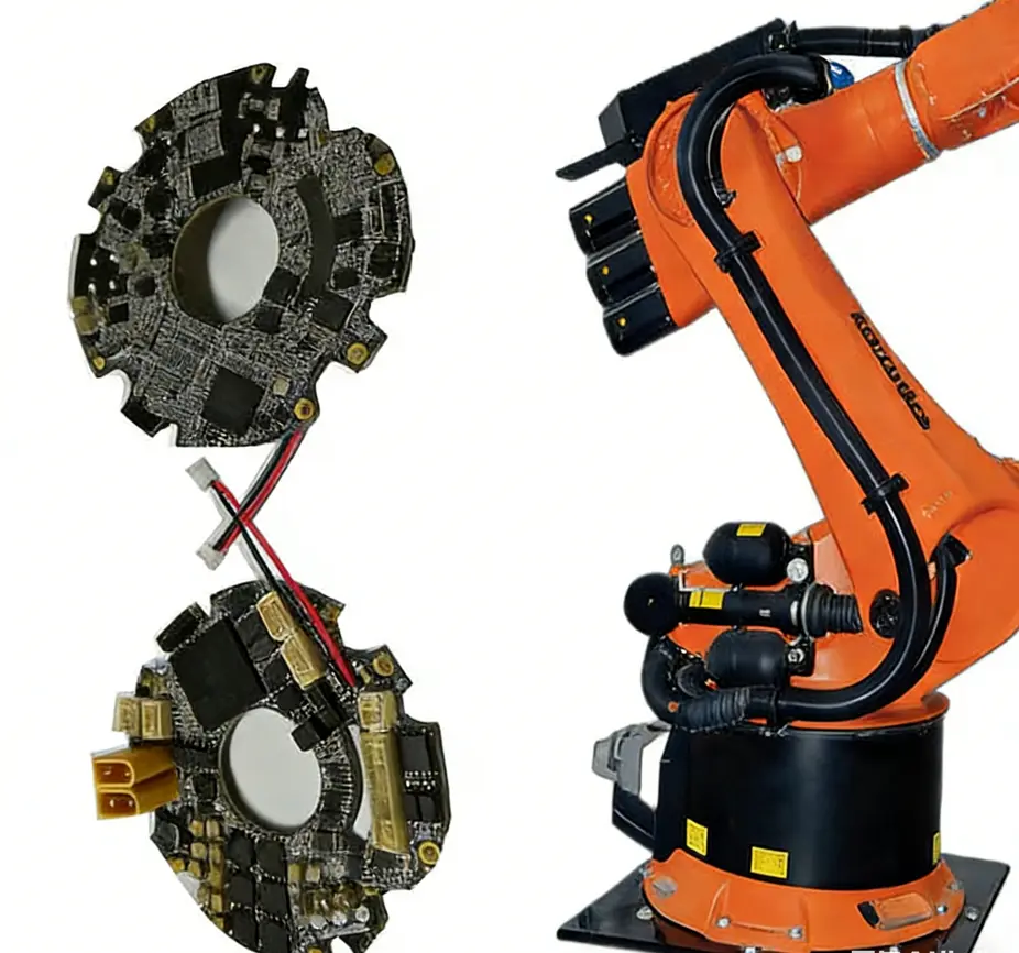
While this technique increases fabrication complexity, it yields PLC boards with superior ruggedness—particularly valuable in mobile robotics or aerospace automation.
Laser Direct Structuring enables the creation of three-dimensional molded interconnect devices (3D-MIDs), where conductive traces are laser-patterned onto thermoplastic substrates. Though not yet mainstream for full PLC boards, LDS is gaining traction for hybrid sensor-integrated control modules:
· Space Efficiency: Combines mechanical housing and circuitry in one part.
· Shock Resistance: No fragile solder joints between separate PCBs and enclosures.
· Custom Geometry: Allows conformal electronics that fit into compact or irregular spaces.
Future PLC designs may leverage 3D-MID for I/O modules or edge-computing nodes requiring both structural and electronic functions.
Durability begins with defect-free manufacturing. Advanced inspection and testing protocols ensure every board meets stringent reliability standards:
· AOI Systems: Use high-resolution cameras and AI algorithms to detect micro-cracks, misaligned vias, or insufficient solder paste—defects that could lead to field failures.
· Flying Probe and ICT: Validate electrical continuity, component values, and isolation resistance before shipment.
· Thermal Cycling and HALT Testing: Accelerated life testing simulates years of thermal stress in hours, identifying weak points in design or assembly.
Integrating these quality controls into the production line minimizes infant mortality and ensures consistent durability across batches.
Beyond fabrication techniques,design philosophy critically influences durability. Modern PLC boards benefit from:
· Thermal Via Arrays: Strategically placed to channel heat from hotspots to ground planes or heatsinks.
· Strain Relief Features: Rounded corners, reinforced mounting holes, and flexible-rigid transitions reduce mechanical stress.
· Creepage and Clearance Optimization: Prevents arcing in high-humidity or high-voltage environments.
Collaboration between design engineers and manufacturing experts during the DFM phase ensures that theoretical durability translates into real-world performance.
The durability of PLC boards in today’s industrial landscape is no longer guaranteed by conventional PCB practices alone. Instead, it emerges from a synergistic integration of advanced materials, precision fabrication techniques, protective coatings, and intelligent design. From HDI architectures and polyimide substrates to parylene conformal coatings and embedded components, each innovation addresses specific failure modes—thermal fatigue, corrosion, vibration, or electrical degradation.
As Industry 4.0 and IoT drive the deployment of PLCs in increasingly remote, uncontrolled, or extreme environments, these advanced manufacturing methods will become standard rather than optional. Manufacturers who invest in these technologies not only extend product lifespans but also reduce total cost of ownership through lower maintenance, fewer replacements, and higher system availability.
For engineers and procurement specialists specifying PLC hardware, understanding these manufacturing advancements is essential to selecting systems that deliver both performance and resilience—now and in the decades ahead.
© 2026 Industrial Automation Insights.PCBMOAll rights reserved.Author: David
· Substrate Material: FR-4 (Flame Retardant Grade 4) epoxy resin glass cloth, TG ≥ 130°C (standard grade), TG ≥ 170°C (high-reliability industrial grade)
· Substrate Thickness: 0.8mm, 1.0mm, 1.6mm (common specifications), tolerance ±0.05mm
· Copper Foil Thickness: 1oz (35μm), 2oz (70μm) for power traces, tolerance ±5μm
· Number of Layers: 2-layer (basic PLC), 4-layer/6-layer (high-performance PLC with complex logic control)
· Surface Finish: ENIG (Electroless Nickel Immersion Gold) – corrosion resistance, good solderability; HASL (Hot Air Solder Leveling) – cost-effective for general applications
· Minimum Trace Width: 0.1mm (4mil) for signal traces, 0.5mm (20mil) for power/ground traces
· Minimum Trace Spacing: 0.1mm (4mil) between adjacent signal traces, 0.5mm (20mil) for high-voltage traces
· Minimum Via Size: Drill diameter 0.2mm (8mil), pad diameter 0.4mm (16mil)
· Annular Ring: ≥ 0.1mm (4mil) to ensure reliable connection and prevent copper peeling
· Clearance to Board Edge: ≥ 0.5mm to avoid damage during cutting and assembly
· Assembly Technology: SMT (Surface Mount Technology) for most components; THT (Through-Hole Technology) for connectors, power terminals and high-power components
· Solder Paste: Lead-free solder paste (Sn96.5Ag3.0Cu0.5, SAC305) compliant with RoHS and REACH regulations
· Reflow Soldering Profile: Peak temperature 245±5°C, dwell time at ≥217°C: 60-90 seconds, total process time: 3-5 minutes
· Wave Soldering Parameters (for THT): Conveyor speed 1.0-1.5m/min, solder temperature 260±5°C, immersion depth 0.5-1.0mm
· Component Placement Accuracy: ±0.05mm for 0402 and smaller SMT components; ±0.1mm for larger components (QFP, BGA)
· Insulation Resistance: ≥ 10^9 Ω at 500V DC between adjacent circuits and circuit to board ground
· Dielectric Withstand Voltage: 1500V AC for 60 seconds (no breakdown, no arcing) for high-voltage sections; 500V AC for 60 seconds for low-voltage signal sections
· Thermal Cycling Test: -40°C to +85°C, 1000 cycles, each cycle 30 minutes (15 minutes heating, 15 minutes cooling), no functional failure or solder joint cracking
· Vibration Test: 5-500Hz, acceleration 10G, X/Y/Z three axes, 2 hours per axis, no component loosening or performance degradation
· Humidity Test: 85% RH, 85°C, 1000 hours (THB test), no corrosion, no insulation performance decline
· ICT (In-Circuit Test): 100% coverage of component continuity, open/short circuit and component value verification
· Board Overall Dimensional Tolerance: ±0.1mm for boards ≤ 200mm × 200mm; ±0.2mm for larger boards
· Solder Joint Appearance: Bright and smooth surface, no cold solder, bridging, voids (void rate ≤ 5% for BGA solder joints), tin beads or solder cracks
· Component Alignment: No obvious tilt (tilt angle ≤ 5°), no component missing, reversed polarity or wrong placement
· Cleanliness: Ion residual ≤ 1.5μg NaCl/cm², no visible flux residue, dust or contaminants after cleaning
· Marking: Clear and durable silk screen marking (component designators, polarity marks, board version), resistant to wiping and environmental aging