PCBA")
 PCBA")
Medical Device PCBs/PCBA: Complete Guide to Design, Standards, Regulations & Applications for OEMs
Medical device PCBs and PCBA serve as the core components underpinning life-saving and diagnostic equipment, necessitating unparalleled reliability, precision, and regulatory compliance. For original equipment manufacturers (OEMs), proficiency in the design principles, industry standards, regulatory frameworks, and application-specific requirements of medical device PCBs/PCBA is paramount to developing safe, effective, and market-viable products. This comprehensive guide delineates key essentials to streamline the product development lifecycle.
Medical Device PCB/PCBA Design Considerations for OEMs
The design of medical device PCBs/PCBA differs substantially from that of consumer electronics, as component failures may result in severe adverse health consequences. OEMs must prioritize the following design parameters to ensure optimal performance and patient safety.
Reliability & Durability Design
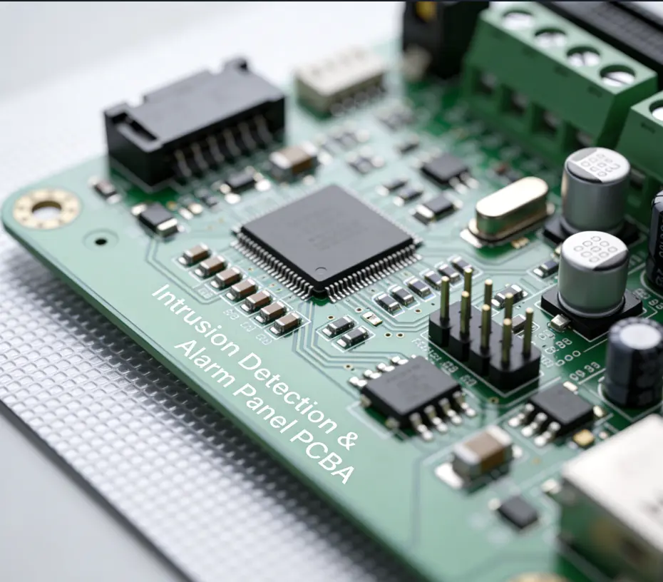
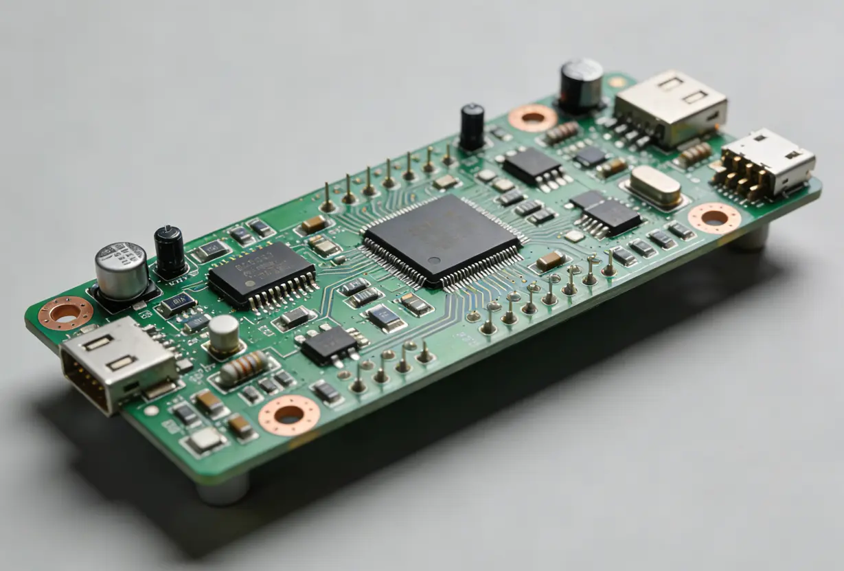
Medical devices, particularly life-support systems and implantable devices, require continuous 24/7 operational capability. PCB design must incorporate robust thermal management solutions to accommodate sustained workloads, as thermal degradation can compromise component integrity. High-quality substrates such as FR-4 are recommended for non-implantable devices, while biocompatible materials are mandatory for implantables to withstand harsh medical environments, including sterilization protocols (autoclaving, ethylene oxide treatment). Controlled impedance is additionally critical for diagnostic equipment to preserve signal integrity during data transmission processes.
Miniaturization & Integration
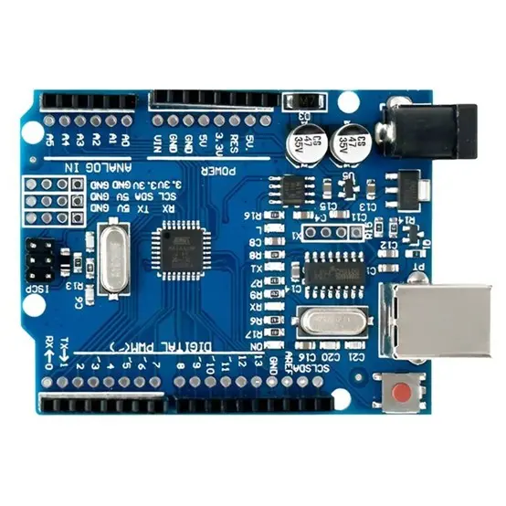
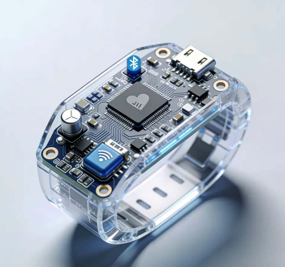
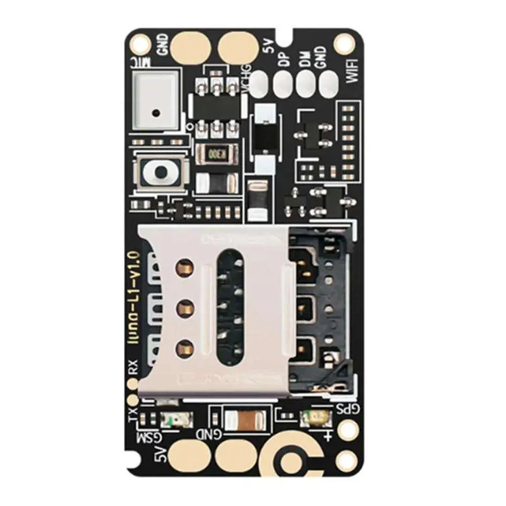
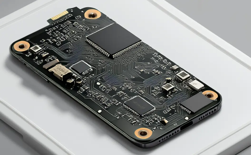
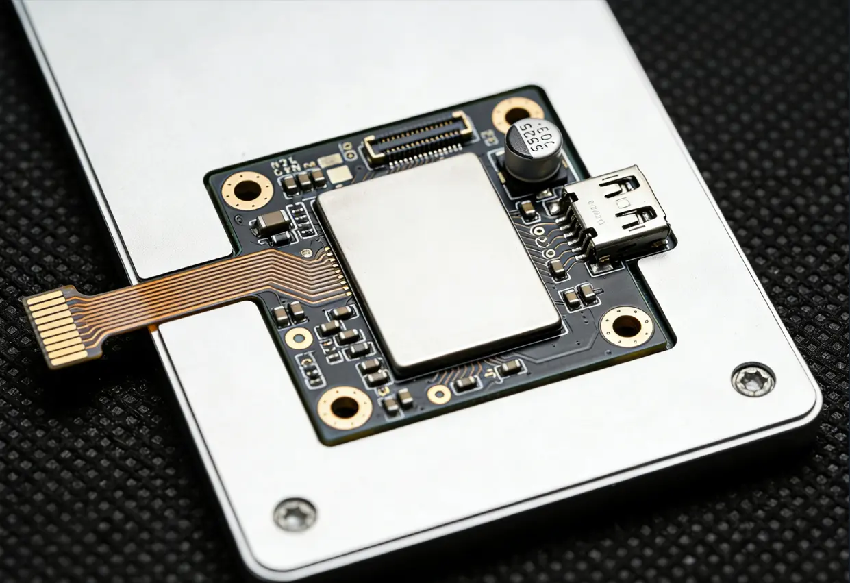
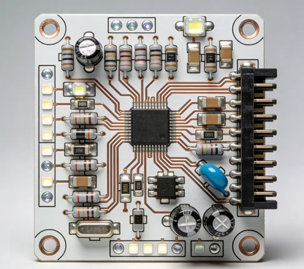
Portable and wearable medical devices (e.g., blood glucose monitors, cardiac monitoring devices) require compact PCB configurations. HDI PCBs (High-Density Interconnect) facilitate higher component density within minimized footprints, enabling complex functionality without sacrificing form factor. Rigid-flex PCBs are well-suited for devices requiring mechanical flexibility (e.g., endoscopes) while maintaining structural rigidity, integrating the advantages of rigid substrates for component mounting and flexible layers for spatial adaptability.
Signal Integrity & EMI Shielding
Diagnostic equipment such as MRI and CT scanners depends on precise signal transmission for accurate results. PCB design must mitigate electromagnetic interference (EMI) through optimized grounding, trace routing, and shielding methodologies. This safeguards against signal degradation and cross-talk, ensuring diagnostic accuracy and compliance with electromagnetic compatibility (EMC) standards.
Key Standards for Medical Device PCBs/PCBA
Adherence to industry standards is imperative for medical device PCBs/PCBA, as these standards establish definitive benchmarks for quality, reliability, and performance. OEMs must align their processes with the following core standards:
IPC Standards
IPC standards are globally acknowledged as the benchmark for electronic assemblies. For medical devices, IPC Class 3 certification is mandatory for high-risk applications (e.g., implantables, life-support systems), mandating stringent manufacturing controls, zero-defect protocols, and comprehensive testing. IPC-6012 (for rigid PCBs) and IPC-6013 (for flexible/rigid-flex PCBs) outline performance specifications, while IPC-A-610 defines acceptability criteria for electronic assemblies, ensuring consistent quality across production lots <superscript:4>.
Material & Manufacturing Standards
Substrate materials must comply with biocompatibility and thermal resistance standards. FR-4 is widely utilized for non-implantable devices, while PTFE and polyimide are preferred for high-temperature or flexible applications. All materials must adhere to RoHS regulations, which restrict the use of hazardous substances such as lead and mercury.
Regulatory Requirements for Medical Device PCBs/PCBA
Regulatory compliance ensures medical devices meet established safety and efficacy criteria. OEMs must navigate regional regulatory frameworks to commercialize their products globally:
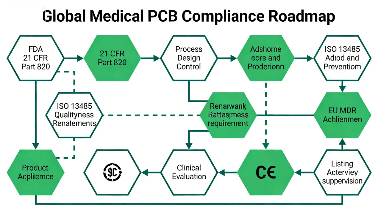
FDA (United States)
The U.S. Food and Drug Administration (FDA) classifies medical devices into Class I, II, or III based on risk profile. PCBs/PCBA for Class II and III devices (e.g., pacemakers, MRI systems) require exhaustive documentation, including design controls, manufacturing process validation, and full traceability records. FDA-approved medical PCBs/PCBA must demonstrate compliance with 21 CFR Part 820 (Quality System Regulation) <superscript:3>.
ISO Regulations
ISO 13485 serves as the primary quality management system standard for medical devices, encompassing PCB/PCBA design, manufacturing, testing, and post-market surveillance. Certification to ISO 13485 is a prerequisite for market access in most global regions, demonstrating a commitment to consistent quality and rigorous risk management <superscript:1>.
EU MDR & Other Regional Regulations
The European Union Medical Device Regulation (EU MDR) mandates that medical device PCBs/PCBA meet stringent traceability and clinical data requirements. Other regional authorities, including Canada’s Health Canada and Japan’s Pharmaceuticals and Medical Devices Agency (PMDA), maintain regulatory frameworks aligned with ISO and IPC standards, with a primary focus on patient safety and product reliability.
Medical Device PCBs/PCBA Applications for OEMs
Medical device PCBs/PCBA power a diverse range of healthcare equipment, each with unique design and performance specifications. The following are key application categories:
In Vitro Diagnostic (IVD) Equipment
In Vitro Diagnostic (IVD) devices, such as blood cell analyzers, chemiluminescence analyzers, and glucose monitors, rely on high-precision PCBs/PCBA for sample analysis and data processing. These PCBs must support high-speed signal transmission and accurate sensor integration to ensure reliable diagnostic outcomes <superscript:1>.
Imaging & Diagnostic Equipment
Advanced imaging devices (X-ray, CT, MRI, ultrasound systems) require PCBs/PCBA capable of handling high-voltage signals and complex data processing workflows. HDI PCBs and rigid-flex assemblies are commonly deployed in these applications to support miniaturization and high-performance requirements, while EMI shielding ensures optimal image clarity <superscript:3>.
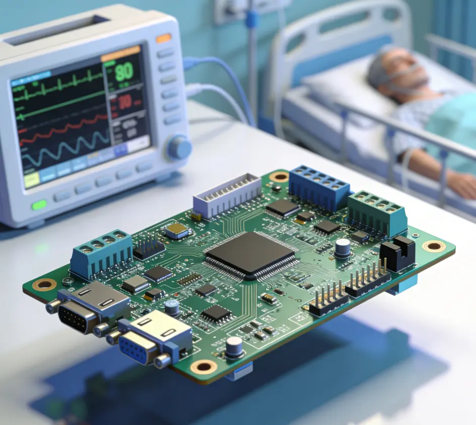
Patient Monitoring & Life-Support Equipment
ECG machines, patient monitors, and anesthesia delivery systems utilize PCBs/PCBA to enable real-time vital sign monitoring and life-sustaining functionalities. These PCBs must comply with IPC Class 3 standards, incorporating redundant design elements to prevent operational failures and ensure uninterrupted performance <superscript:4>.
Home Medical Equipment
Portable home medical devices (sphygmomanometers, nebulizers, wearable fitness monitors) require cost-effective, compact PCBs/PCBA with low power consumption profiles. Flexible PCBs are optimal for wearable applications, conforming to body contours while maintaining structural reliability <superscript:1>.
Manufacturing & Quality Control for Medical PCBs/PCBA
OEMs must collaborate with manufacturers (such as PCBMO) specializing in medical-grade PCBs/PCBA, equipped with rigorous quality control protocols. Key manufacturing considerations include full traceability (from material sourcing to final delivery), automated optical inspection (AOI) for defect detection, and environmental testing (temperature, humidity, vibration) to validate performance under real-world operating conditions.
Emerging Trends in Medical Device PCBs/PCBA
The medical PCB/PCBA sector is evolving in tandem with technological advancements, including the integration of Internet of Things (IoT) capabilities for remote patient monitoring, the miniaturization of implantable devices, and the adoption of advanced materials to enhance biocompatibility. OEMs must remain abreast of these trends to develop innovative, market-competitive products.
By prioritizing design best practices, adhering to stringent standards and regulatory requirements, and understanding application-specific demands, OEMs can develop medical devices powered by reliable, compliant PCBs/PCBA. Partnering with a specialized manufacturer like PCBMO ensures access to medical-grade production expertise, facilitating seamless compliance and product commercialization success.
PCB Fabrication Parameters
Layer Count: 2 to 12+ layers (commonly 4–8 for mid-to-high complexity IVD devices)
Board Thickness: 0.8 mm to 2.0 mm (standard: 1.6 mm)
Base Material: FR-4 (standard), High-Tg FR-4, or specialized materials (e.g., Rogers for RF modules)
Copper Weight: 0.5 oz to 2 oz (typically 1 oz for signal layers, 2 oz for power planes)
Minimum Trace/Space: 4/4 mil (100 µm) or finer for high-density designs
Hole Size (Drilled): ≥0.15 mm (mechanical), laser microvias down to 0.075 mm for HDI
Surface Finish:
ENIG (Electroless Nickel Immersion Gold) – most common for IVD (good solderability, shelf life)
Immersion Silver / Tin
HASL (Lead-free) – less common due to flatness concerns
Solder Mask: Liquid Photoimageable (LPI), color typically green, but white/black for optical modules
Silkscreen: White or contrasting color for clear labeling
Component Assembly & SMT Parameters
Component Types Supported:
01005 (0402 metric) to large BGAs, QFNs, connectors, through-hole components
Mixed technology (SMT + THT)
Placement Accuracy: ±25 µm or better (for fine-pitch BGAs/QFNs)
Reflow Profile: Lead-free (SAC305 alloy), peak temp ~240–250°C, controlled ramp/cooling rates
Wave Soldering (for THT): Nitrogen-enriched, selective soldering preferred for reliability
X-ray Inspection: For BGA, CSP, and hidden solder joints (AXI)
Automated Optical Inspection (AOI): Pre- and post-reflow
Cleaning & Conformal Coating (Critical for IVD)
Cleaning Process: Aqueous or semi-aqueous cleaning to remove flux residues (IPC-J-STD-001 Class 3)
Ionic Contamination: <1.56 µg NaCl/cm² (per IPC TM-650 2.3.28)
Conformal Coating Type:
Acrylic (most common – easy rework)
Urethane (chemical/moisture resistance)
Silicone (flexible, wide temp range)
Coating Thickness: 25–75 µm (per IPC-CC-830)
Selective Coating: Masking of connectors, test points, and optical windows
Quality & Compliance Standards
Acceptability Standard: IPC-A-610 Class 3 (High Performance Electronics)
Soldering Standard: IPC-J-STD-001 Class 3
Traceability: Full component lot traceability (UDI-compliant where applicable)
ESD Control: ANSI/ESD S20.20 compliant manufacturing environment
Cleanliness: Verified per IEC 60601-1 (medical electrical equipment safety)
Testing & Validation
In-Circuit Test (ICT): Bed-of-nails or flying probe for shorts/opens, component values
Functional Test (FCT): Simulated operational conditions (e.g., sensor input, communication)
Boundary Scan (JTAG): For complex digital logic
Environmental Stress Screening (ESS): Thermal cycling, humidity exposure (optional per design validation)
Burn-in Testing: For high-reliability or long-life IVD systems
Regulatory & Documentation Requirements
RoHS/REACH Compliance: Lead-free, halogen-free options available
Material Declaration: IPC-1752A format for substance reporting
Manufacturing Records: Retained per ISO 13485 (typically 10+ years)
Design for Manufacturing (DFM) / Design for Test (DFT): Reviewed prior to production