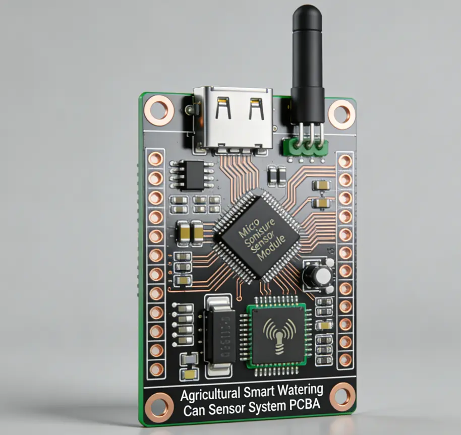
Welcome your arrival!

Welcome your arrival!

Battery Management System (BMS) PCBA Number of Layers:2–8 layers (commonly 4 layers)
Base Material:FR-4 (high Tg for high-temperature environments), aluminum-core PCB (for high thermal dissipation)
Copper Thickness:1 oz – 2 oz (1 oz typical for signal layers; power layers may be thicker)
Minimum Trace Width/Spacing:≥0.15 mm (6 mil)
Hole Diameter Tolerance:±0.05 mm
Surface Finish:ENIG (Electroless Nickel Immersion Gold), HASL (lead-free or leaded), OSP
Impedance Control:Required for high-speed communication (e.g., CAN); e.g., 120Ω differential
Product Details Data Sheet

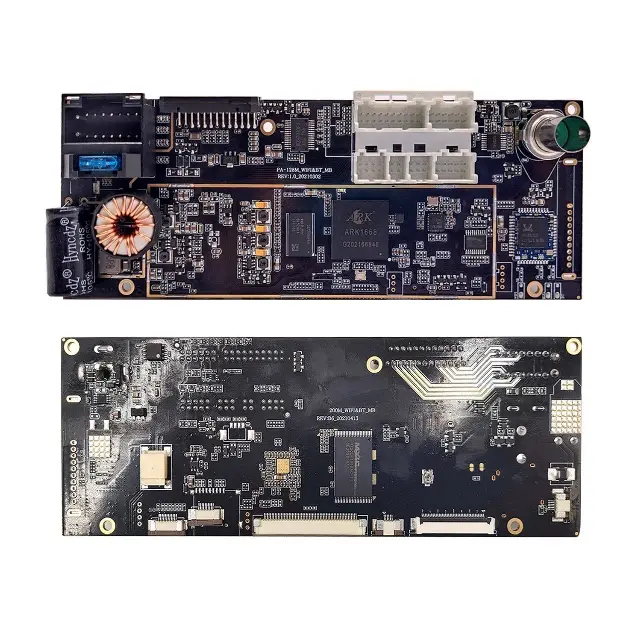
Battery Management System (BMS) PCBA: Design, Assembly, and Protection for Lithium Battery Applications

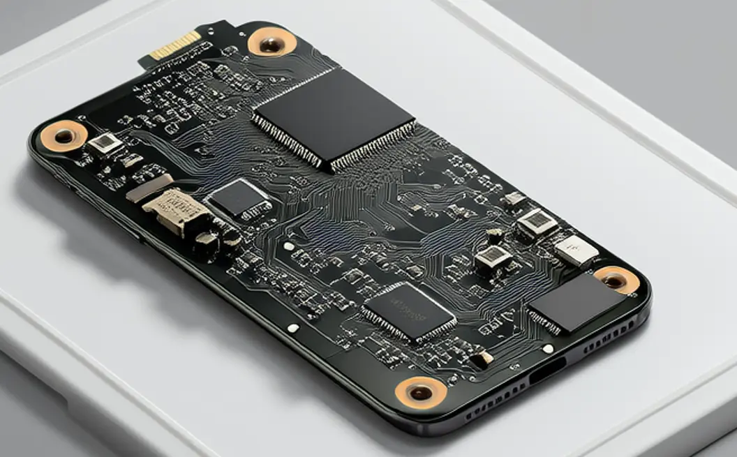
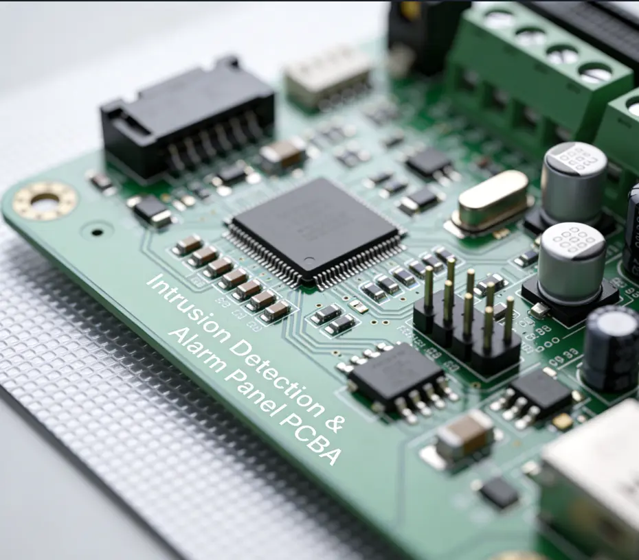
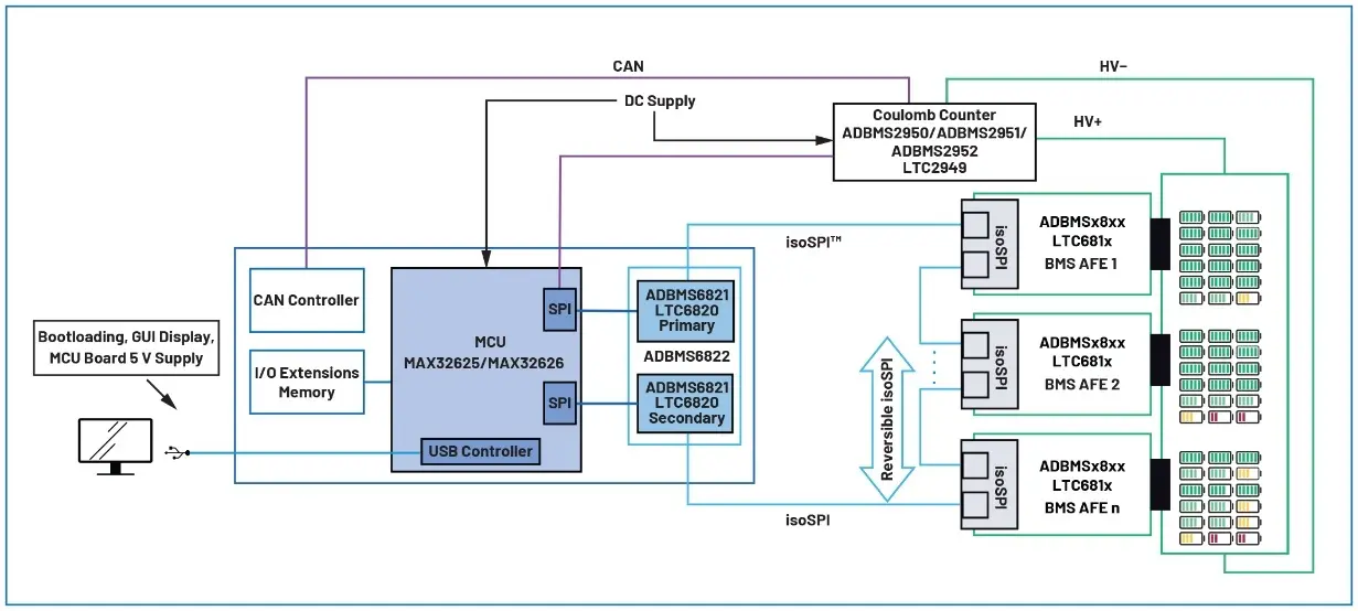
In the era of electrification—spanning electric vehicles (EVs), renewable energy storage, consumer electronics, and industrial power tools—the Battery Management System (BMS) has emerged as the central nervous system of any lithium-based battery pack. At the heart of every BMS lies its physical embodiment: the Battery Management System PCBA (Printed Circuit Board Assembly). This critical component integrates sensing, control, communication, and safety mechanisms into a compact, reliable platform. In this article, we delve into the architecture, manufacturing considerations, functional roles, and evolving trends of BMS PCBA, with special emphasis on BMS PCB Assembly, BMS Protection Board PCBA, and their indispensable role in modern Lithium Battery BMS PCBA applications.


What Is a BMS PCBA?
A BMS PCBA is not merely a circuit board—it is a sophisticated electro-mechanical subsystem responsible for monitoring, managing, and safeguarding rechargeable lithium-ion or lithium iron phosphate (LiFePO₄) battery packs. Unlike generic PCBs, a BMS PCB Assembly must operate reliably under harsh electrical and thermal conditions while delivering millivolt-level precision in voltage and current measurements.
The core functions of a typical Battery Management System PCBA include:
  • Cell voltage and temperature monitoring
  • State-of-Charge (SoC) and State-of-Health (SoH) estimation
  • Overvoltage, undervoltage, overcurrent, and short-circuit protection
  • Cell balancing (passive or active)
  • Communication with external systems (via CAN, UART, etc.)
  • Thermal management coordination

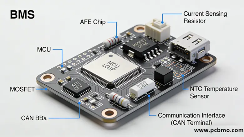
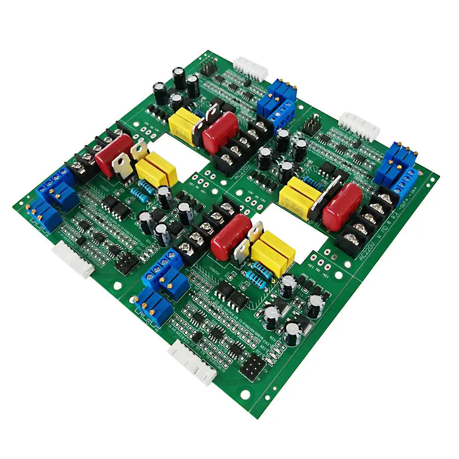
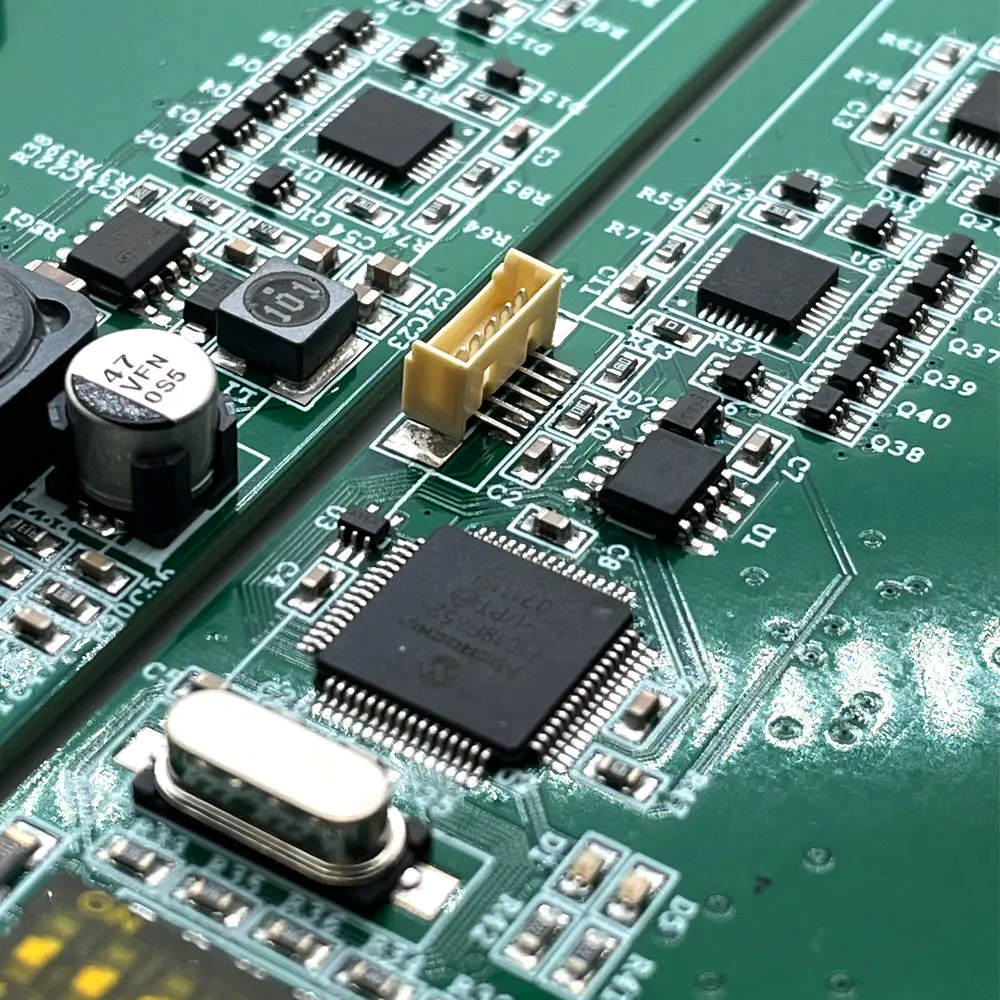
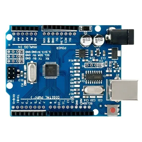
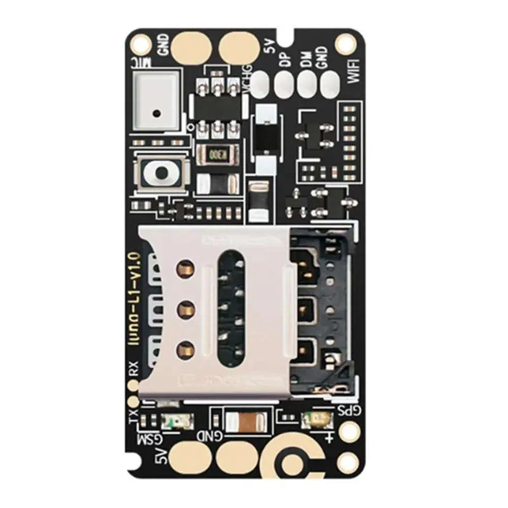
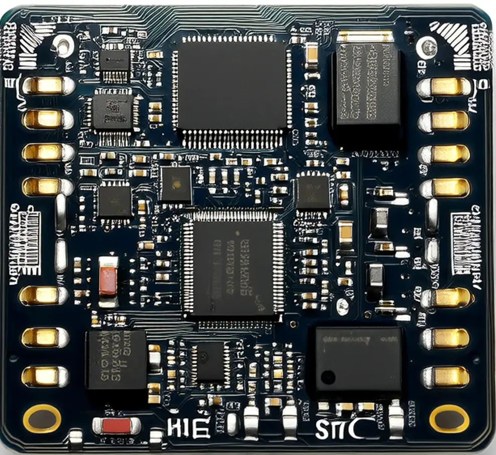
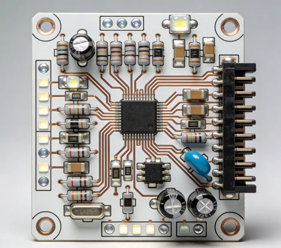
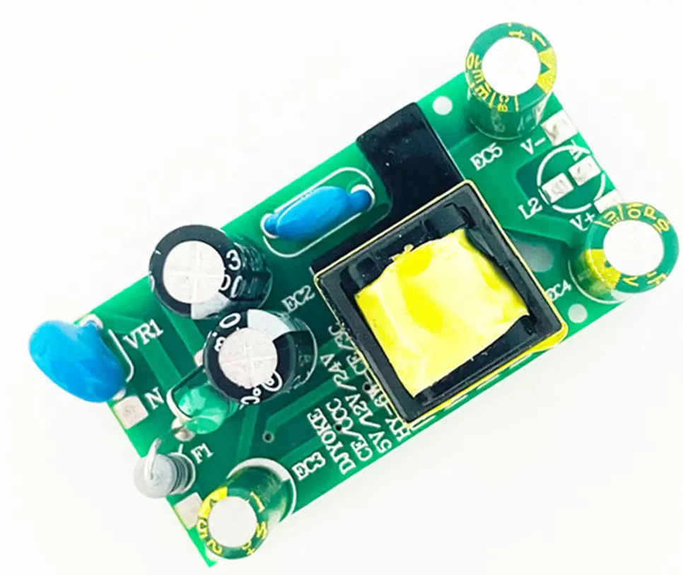
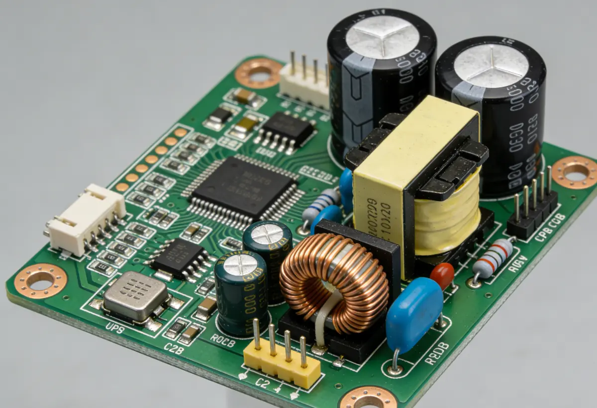
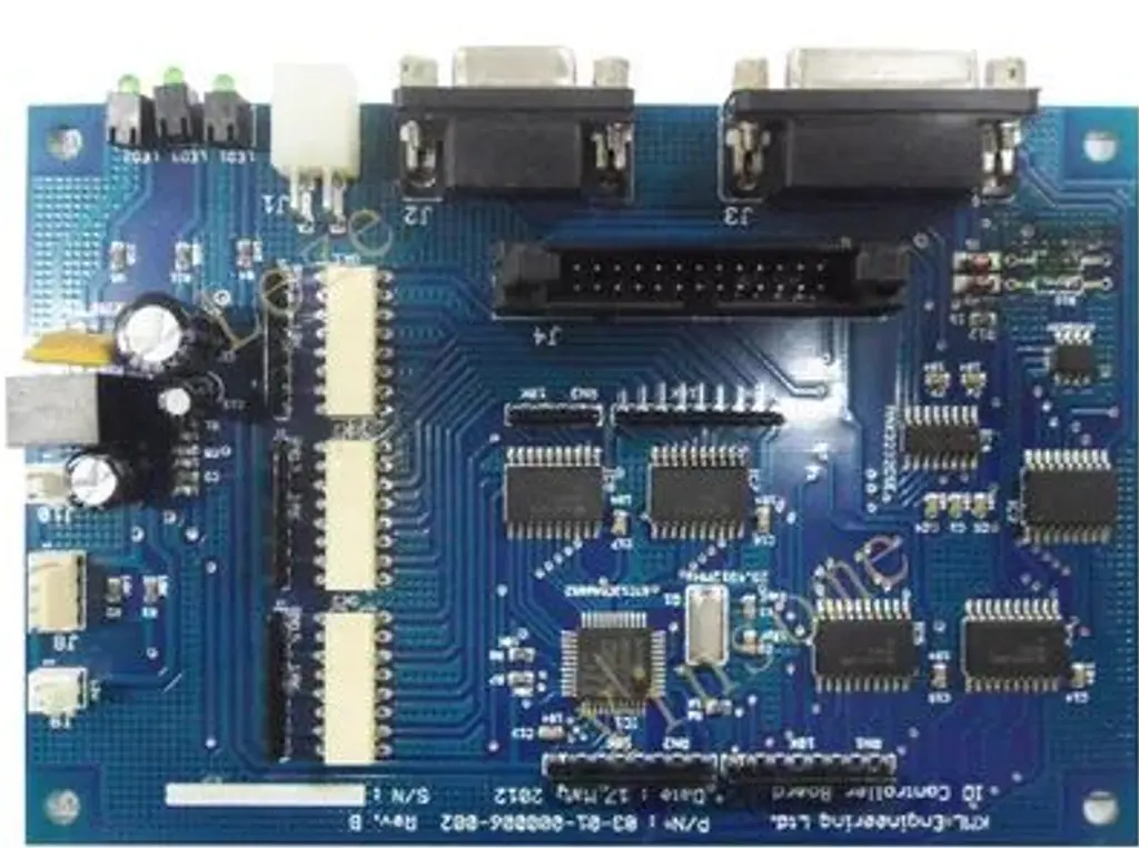
These functions are implemented through a combination of analog front-end (AFE) ICs, microcontrollers (MCUs), MOSFETs, shunt resistors, and isolation components—all mounted on a carefully designed PCB that undergoes rigorous BMS PCB Assembly processes.


The Role of the BMS Protection Board PCBA
One of the most vital aspects of any Lithium Battery BMS PCBA is its integrated protection circuitry. Often referred to as the BMS Protection Board PCBA, this subsystem acts as the last line of defense against catastrophic failures such as thermal runaway, fire, or explosion.
The BMS Protection Board PCBA typically includes:
  • High-accuracy voltage monitoring ICs (e.g., TI BQ769x0, NXP MC3377x)
  • Dual N-channel MOSFETs for charge/discharge path control
  • Fuses or PTC devices for secondary overcurrent protection
  • ESD and surge suppression components
  • Redundant safety logic (hardware + firmware)
For example, in a 12S (12-series) LiFePO₄ battery pack used in solar energy storage, the BMS Protection Board PCBA continuously checks each cell’s voltage. If any cell exceeds 3.65V (overvoltage threshold) or drops below 2.5V (undervoltage), the BMS immediately disconnects the load or charger via MOSFET switching—preventing irreversible damage.
This protective intelligence is embedded directly into the BMS PCBA during the BMS PCB Assembly phase, where component placement, solder joint integrity, and signal integrity are paramount.

Key Considerations in BMS PCB Assembly
Manufacturing a high-reliability Battery Management System PCBA demands more than standard SMT (Surface Mount Technology) practices. Due to the high-voltage, high-current, and safety-critical nature of BMS applications, the BMS PCB Assembly process must adhere to stringent quality and design standards.
1. PCB Material and Layer Stackup
Most Lithium Battery BMS PCBA designs use FR-4 with high Tg (glass transition temperature >170°C) to withstand thermal stress. For high-power applications (e.g., EVs), metal-core PCBs (aluminum-backed) may be employed to dissipate heat from MOSFETs and shunt resistors.
A typical BMS PCBA uses 4–6 layers:
  • Top/Bottom: Signal and component placement
  • Inner Layer 1: Ground plane (for noise reduction)
  • Inner Layer 2: Power plane (for clean VCC distribution)

2. Component Selection and Placement
Precision is non-negotiable. Voltage sense traces must be Kelvin-connected to avoid measurement errors. High-voltage (>60V) and low-voltage (<5V) sections must be physically separated with creepage/clearance distances compliant with IEC 62133 or UL 60730.
Critical components like AFE ICs, NTC thermistors, and current shunts are placed close to battery terminals to minimize trace resistance and inductance.
3. Soldering and Inspection
Lead-free reflow profiles (e.g., SAC305 alloy) are standard. However, due to mixed packages (QFN, SOIC, large MOSFETs), thermal profiling must be optimized to prevent tombstoning or voiding.

Automated Optical Inspection (AOI) and X-ray inspection (for QFN thermal pads) are essential to ensure solder joint reliability—especially since field failures in a BMS Protection Board PCBA can have severe safety consequences.


Functional Testing and Validation
After BMS PCB Assembly, every unit undergoes rigorous validation:
  • Cell Voltage Accuracy Test: ±2 mV per cell
  • Current Measurement Calibration: ±0.5% error tolerance
  • Isolation Resistance Test: >100 MΩ at 500V DC
  • Hi-Pot Test: 1.5 kV AC for 60 seconds between high-voltage and logic grounds
  • Communication Protocol Verification: CAN bus message integrity, baud rate accuracy

Only after passing these tests is a Battery Management System PCBA deemed ready for integration into a battery module.


Applications Driving BMS PCBA Innovation
The demand for advanced Lithium Battery BMS PCBA solutions is surging across sectors:
  • Electric Vehicles (EVs): Require automotive-grade (AEC-Q100) BMS PCBA with ASIL-B/C functional safety (ISO 26262).
  • Energy Storage Systems (ESS): Need scalable, modular BMS Protection Board PCBA for 48V–1000V architectures.
  • E-Bikes & Power Tools: Prioritize compact, cost-effective BMS PCB Assembly with robust overcurrent protection.
  • Uninterruptible Power Supplies (UPS): Depend on long-life, low-self-discharge BMS PCBA with accurate SoC tracking.
Each application imposes unique constraints on form factor, cost, safety, and communication—pushing BMS PCBA designers toward greater integration and intelligence.
Future Trends: From Passive to Predictive BMS
The next generation of Battery Management System PCBA is moving beyond reactive protection toward predictive analytics. By integrating machine learning algorithms into the MCU firmware, modern BMS PCBA units can:
  • Forecast remaining useful life (RUL)
  • Detect early signs of internal short circuits
  • Adapt balancing strategies based on usage patterns
  • Communicate health data to cloud platforms via Bluetooth or cellular

Moreover, wireless BMS (wBMS) architectures—pioneered by companies like Analog Devices—are eliminating copper interconnects between cells, reducing weight and improving reliability. However, even in wBMS, a centralized BMS Protection Board PCBA remains essential for master control and fail-safe operations.


Conclusion
The Battery Management System PCBA is far more than a supporting component—it is the guardian, brain, and communicator of modern lithium battery systems. From the precision of its BMS PCB Assembly to the robustness of its BMS Protection Board PCBA, every design decision impacts safety, performance, and longevity. As global reliance on lithium batteries grows, so too does the importance of engineering a Lithium Battery BMS PCBA that is accurate, reliable, and intelligent.
For manufacturers, investing in high-quality BMS PCBA development isn’t optional—it’s a prerequisite for market access, regulatory compliance, and user trust. Whether powering a smartphone or a 400-mile-range EV, the humble BMS PCBA silently ensures that energy is stored, delivered, and protected with uncompromising fidelity.

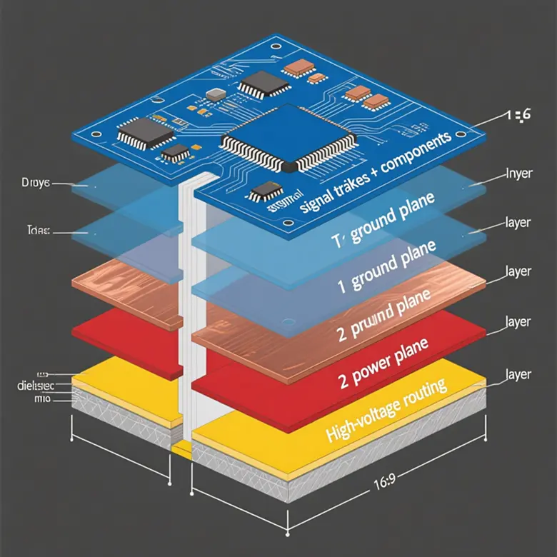
I. PCB Design Parameters

Parameter Category Typical Value / Requirement
Number of Layers 2–8 layers (commonly 4 layers)
Base Material FR-4 (high Tg for high-temperature environments), aluminum-core PCB (for high thermal dissipation)
Copper Thickness 1 oz – 2 oz (1 oz typical for signal layers; power layers may be thicker)
Minimum Trace Width/Spacing ≥0.15 mm (6 mil)
Hole Diameter Tolerance ±0.05 mm
Surface Finish ENIG (Electroless Nickel Immersion Gold), HASL (lead-free or leaded), OSP
Impedance Control Required for high-speed communication (e.g., CAN); e.g., 120Ω differential

II. Key Component Selection Parameters

Component Category Key Specifications
Microcontroller (MCU) Integrated ADC, CAN/LIN support, low-power modes, operating temperature range (-40°C to +125°C)
Cell Voltage Monitoring IC Accuracy ±1–5 mV; channel count (typically 6–16 cells in series)
Current Sensing Shunt resistor or Hall-effect sensor; accuracy ±0.5%–1%
Temperature Sensor NTC/PTC thermistors; accuracy ±1°C
MOSFET Driver Supports high-side/low-side drive; includes overcurrent protection
Communication Interfaces 
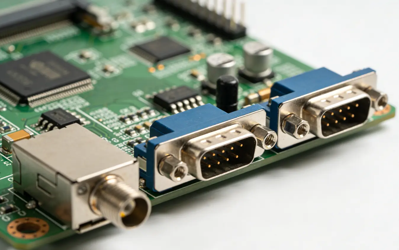
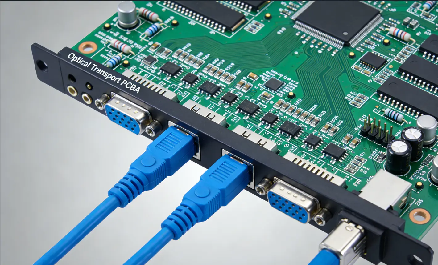
CAN 2.0B, RS485, UART, I²C
Isolation Components Digital isolators (e.g., ISO7741); isolation voltage ≥2.5 kVRMS

III. SMT (Surface Mount Technology) Manufacturing Process Parameters

Process Step Technical Parameters
Placement Accuracy ±0.05 mm (for 0201, QFN, BGA packages)
Reflow Profile Lead-free solder (e.g., SAC305): peak temperature 240–250°C, time above liquidus 30–60 seconds
AOI Inspection Coverage ≥98%; capable of detecting missing components, misalignment, insufficient solder, etc.
X-Ray Inspection Used for inspecting solder joints under BGA/QFN packages
Cleaning Process Optional aqueous cleaning or no-clean (depending on flux type)

IV. Functional and Reliability Test Parameters

Test Item Requirement
Cell Voltage Measurement Accuracy ±2 mV (typical)
Total Pack Voltage Error ≤±0.5%
Current Sensing Bandwidth ≥1 kHz (for dynamic response)
Insulation Resistance ≥100 MΩ (at 500 V DC)
Dielectric Withstand Test 1.5 kV AC for 1 minute (input-output, input-ground)
ESD Protection ±8 kV contact discharge, ±15 kV air discharge (per IEC 61000-4-2)
Operating Temperature Range -40°C to +85°C (industrial grade) or -40°C to +125°C (automotive grade)
Vibration & Shock Compliant with ISO 16750-3 (automotive) or IEC 60068-2 (general)

V. Compliance and Certification Requirements (Application-Dependent)

1、Automotive Grade: AEC-Q100 (ICs), ISO 26262 (functional safety, ASIL level), IATF 16949 (quality management)
2、Industrial / Energy Storage: UL 60730, IEC 62133, UN38.3 (transport safety)
3、Environmental Compliance: RoHS, REACH, halogen-free