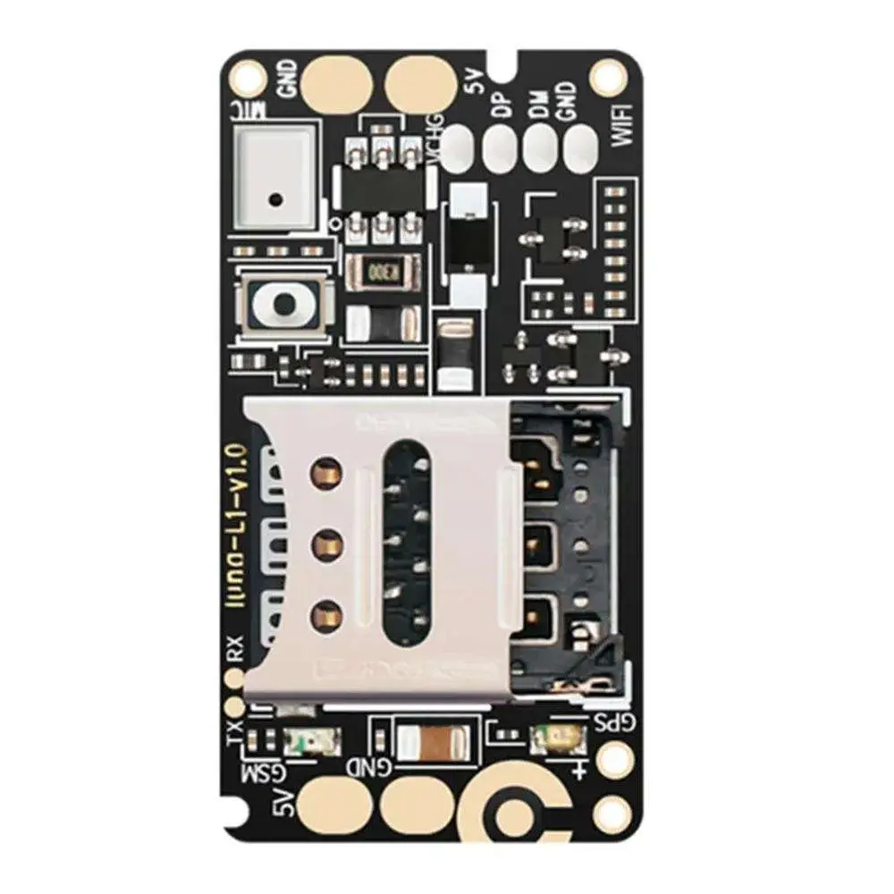
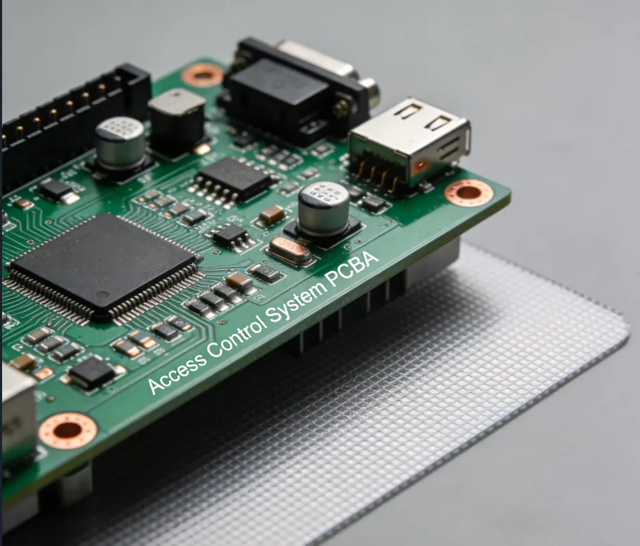
PCBA")
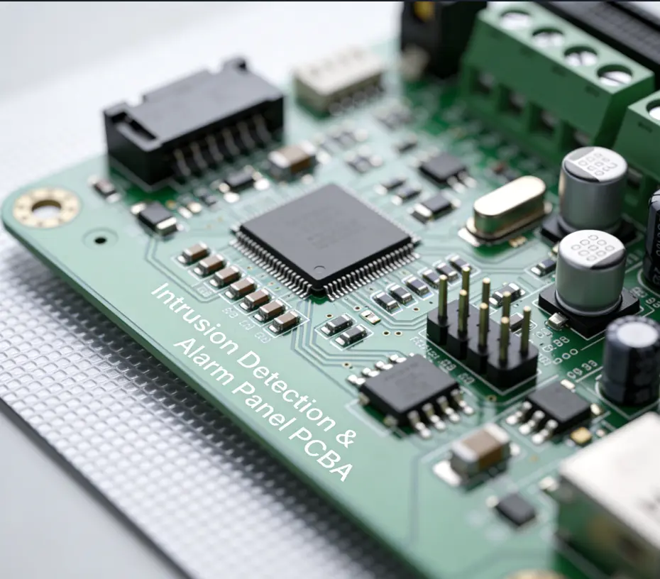
 PCBA")
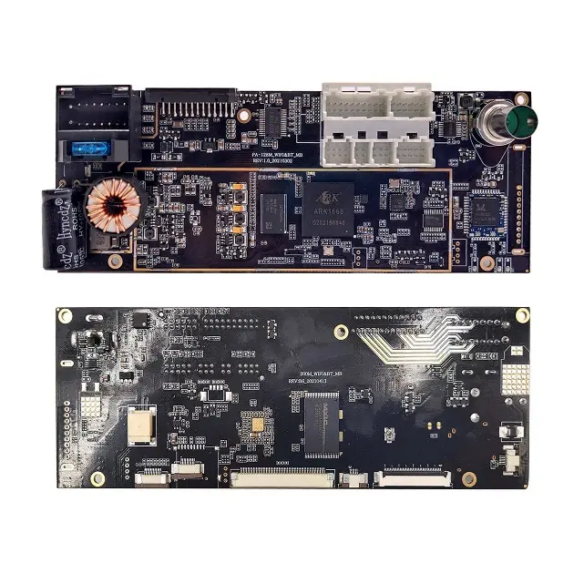
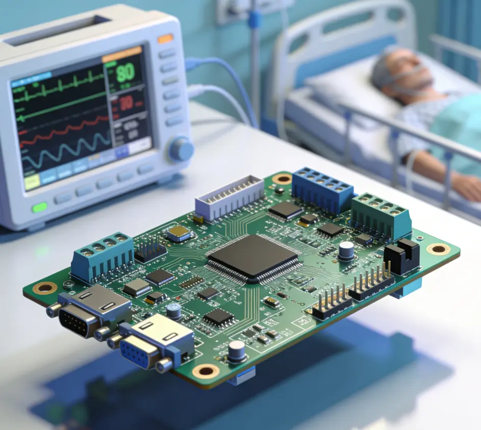
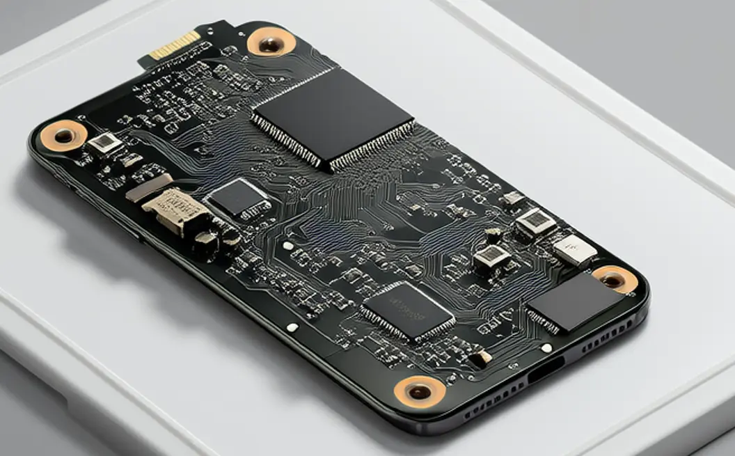
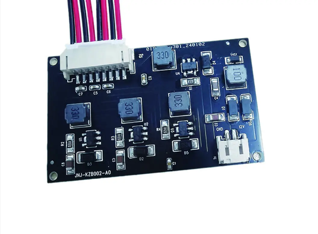
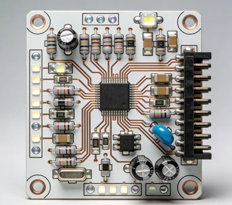
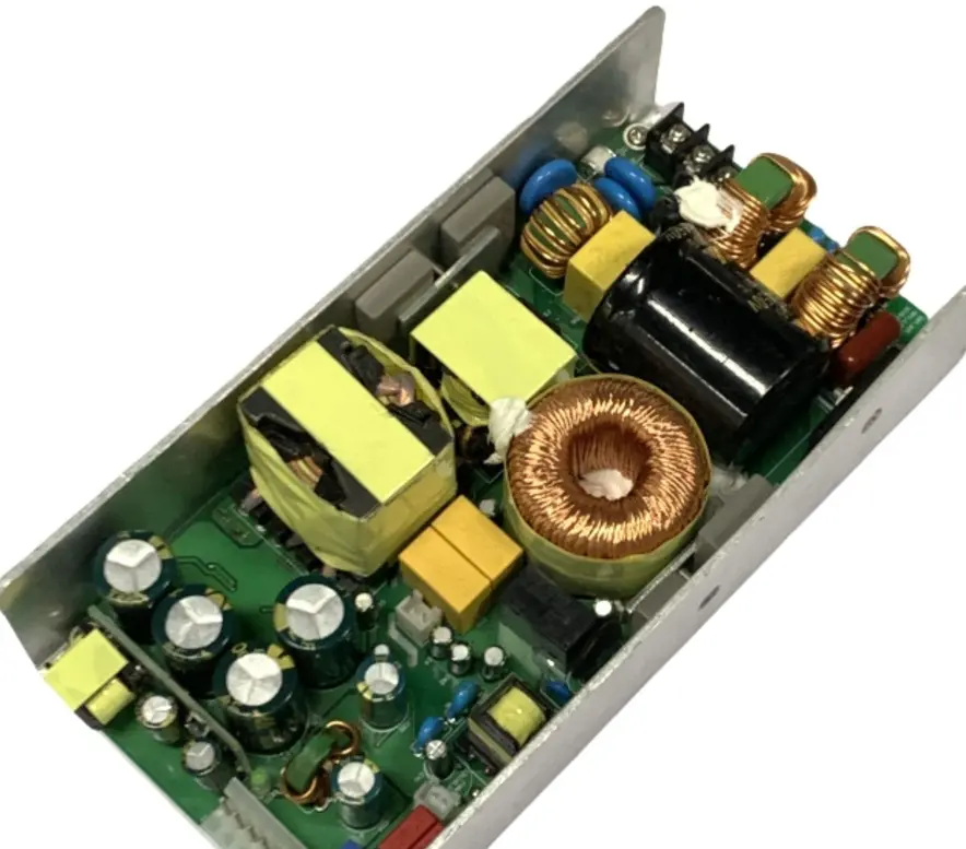
At PCBMO, we bring your high-reliability HMI PCBA visions to life. Leveraging our advanced manufacturing capabilities, we deliver precision-engineered boards—from complex 12-layer industrial designs to ultra-thin consumer modules—with exceptional quality (IPC Class 3 compliant), competitive pricing, and rapid turnaround times. This guide details the critical technical parameters we master to ensure your HMI success.
1. Basic PCB Substrate: The Foundation of HMI PCBA Performance
The PCB substrate serves as the physical and electrical foundation of the HMI PCBA, supporting all components, traces, and conductive paths while providing mechanical rigidity and environmental protection. Choosing the right substrate material and specifications is the first critical step in HMI PCBA manufacturing, as it directly impacts the device’s thermal stability, signal transmission capabilities, and adaptability to harsh operating environments. Below are the core technical parameters and application guidelines for HMI PCB substrates, with a focus on high-impact, high-search-volume terms.
1.1 Core Technical Specifications for HMI PCB Substrates
When selecting a substrate for HMI PCBA, manufacturers must prioritize three key parameters: material type, layer count, and board thickness—each tailored to the specific use case of the HMI device.
1.1.1 Substrate Material: Balancing Performance, Cost, and Environmental Resilience
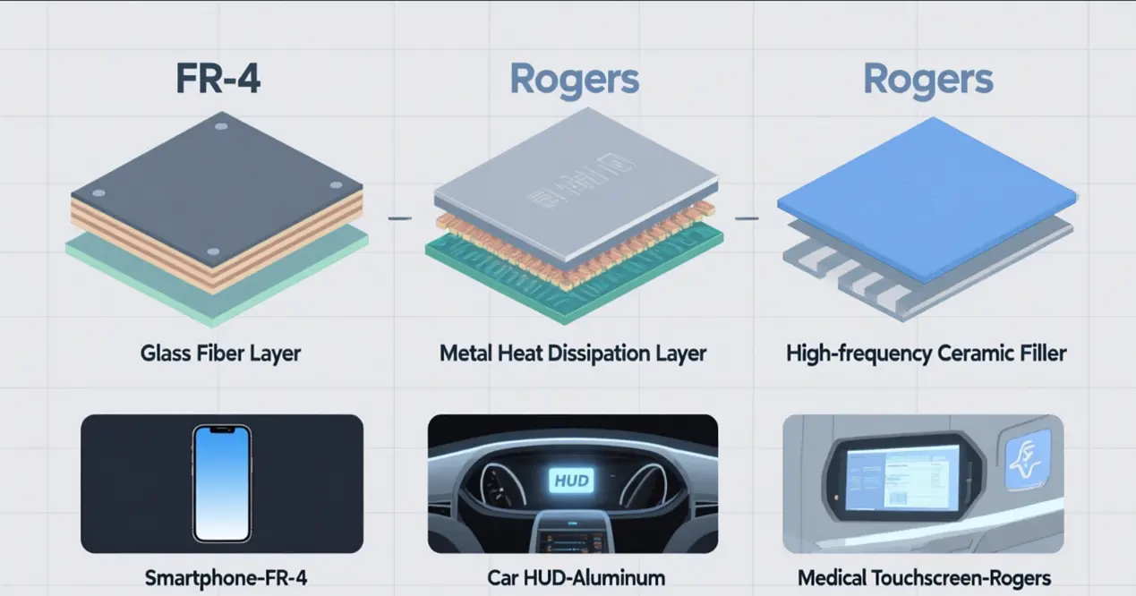
The most commonly used substrate materials for HMI PCBA include FR-4 (flame retardant 4), aluminum PCB for high-heat HMI, and Rogers 4350B for high-frequency touch signal transmission—each with unique properties that make them suitable for different HMI scenarios.
· FR-4 High-Tg Substrate: FR-4 is the workhorse of HMI PCBA manufacturing, thanks to its excellent mechanical strength, electrical insulation, and cost-effectiveness. The key differentiator for HMI applications is the glass transition temperature (Tg), which refers to the temperature at which the substrate transitions from a rigid, glassy state to a soft, rubbery state. For consumer HMI PCBA (such as smartphone touchscreens, tablet displays, and smart home control panels), a Tg of ≥130°C is sufficient to withstand normal operating temperatures and mild thermal stress. For industrial HMI PCBA (used in factory automation, CNC machines, and outdoor monitoring systems) and automotive HMI PCBA (infotainment screens, instrument clusters, and climate control panels), a high-Tg FR-4 (Tg ≥170°C) is mandatory. This higher Tg ensures the substrate maintains its structural integrity and electrical performance under prolonged high-temperature operation, preventing warpage, delamination, and signal degradation—common issues that plague low-Tg substrates in harsh environments.
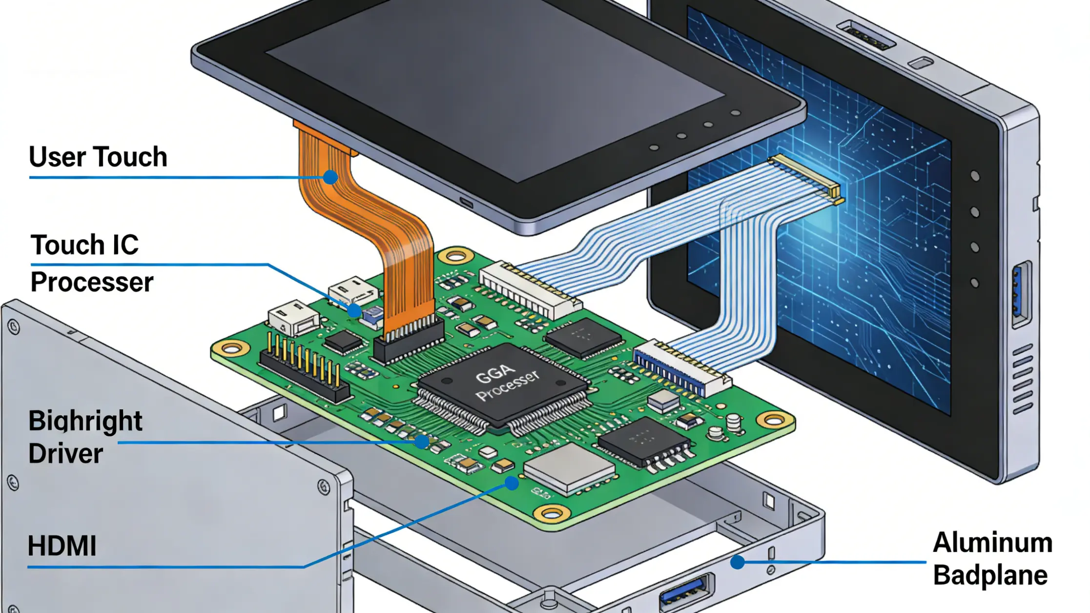
· Aluminum PCB for HMI Backplane Heat Dissipation: Many HMI devices, particularly those with bright backlight modules (such as automotive head-up displays and industrial control panels), generate significant heat during operation. Excessive heat buildup can damage sensitive components like touch ICs and display drivers, leading to reduced lifespan and erratic performance. Aluminum PCB (also known as metal-core PCB or MCPCB) addresses this challenge by integrating a thin aluminum base layer that acts as a passive heat sink, efficiently dissipating heat away from critical components to the surrounding environment. This substrate is primarily used for HMI PCBA backplanes and high-power HMI devices, where thermal management is a top priority. Unlike FR-4, aluminum PCBs offer thermal conductivity values ranging from 1W/mK to 5W/mK (depending on the dielectric layer), making them up to 10 times more effective at heat dissipation than standard FR-4 substrates.
· Rogers 4350B for High-Frequency Touch Signal Integrity: For HMI devices that rely on high-frequency touch signal transmission (such as capacitive touchscreens with multi-touch functionality and high-resolution displays), Rogers 4350B is the gold standard substrate material. This high-frequency laminate offers a low and stable dielectric constant (Dk = 3.48 at 1GHz), low loss tangent (Df = 0.0037 at 1GHz), and excellent dimensional stability—all critical for maintaining touch signal integrity and minimizing signal attenuation, reflection, and crosstalk. Unlike FR-4, which can experience significant Dk variation with temperature and frequency, Rogers 4350B provides consistent electrical performance across the operating range of high-end HMI devices, ensuring that touch inputs are detected accurately and rapidly, even in noisy electromagnetic environments. This makes it ideal for precision HMI PCBA applications such as medical diagnostic equipment, aerospace control panels, and high-end automotive infotainment systems.
1.1.2 PCB Layer Count: Matching Complexity to Application Requirements
The number of PCB layers directly correlates with the complexity of the HMI device’s functionality, as more layers allow for greater component density, improved signal routing, and better isolation between high-current and high-frequency circuits.
· 2–4 Layers for Consumer HMI PCBA: Most consumer HMI devices (smartphones, tablets, smartwatches, and home automation controllers) utilize 2 to 4 layer PCBs. These devices typically have relatively simple functionality, with fewer integrated control modules, and prioritize miniaturization and cost control. A 2-layer PCB is sufficient for basic touchscreens with a single touch IC and backlight driver, while a 4-layer PCB is used for more advanced consumer HMI devices with additional features such as wireless connectivity (Bluetooth, Wi-Fi) and onboard processing. The extra layers in 4-layer PCBs allow for dedicated power and ground planes, which improve power supply noise reduction and signal grounding—critical for maintaining touch sensitivity and display clarity in portable consumer devices.
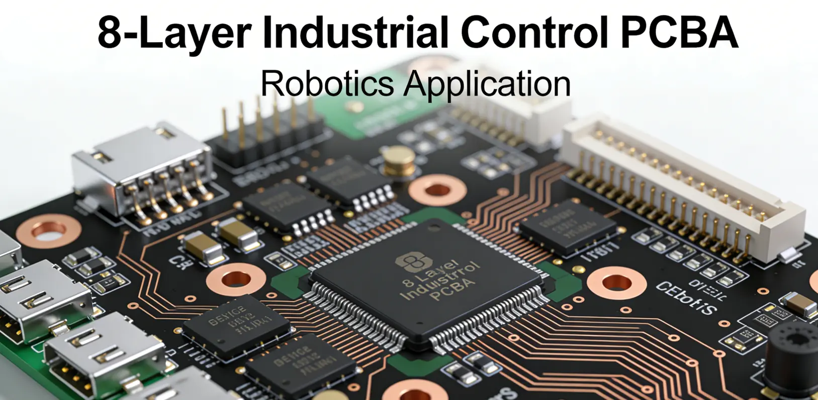
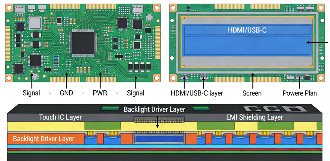
· 6–12 Layers for Industrial/Automotive HMI PCBA: Industrial and automotive HMI devices are far more complex, often integrating multiple control modules, high-power components, high-frequency touch circuits, and communication interfaces (such as USB-C for HMI data transmission, HDMI for HMI display output, and RS485 for industrial HMI communication). As such, they require 6 to 12 layer PCBs to accommodate the dense component layout and complex routing requirements. For example, an automotive infotainment HMI PCBA may include a 10-layer PCB with dedicated layers for touch signal routing, power distribution, ground planes, high-speed data transmission (HDMI/USB-C), and control module integration (engine monitoring, climate control, navigation). The additional layers in these PCBs also provide better thermal management and electromagnetic interference (EMI) shielding, which is essential for operating in the harsh electromagnetic environment of a vehicle or industrial factory floor.
1.1.3 Board Thickness: Balancing Rigidity, Miniaturization, and Thermal Performance
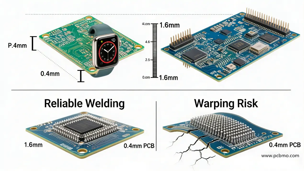
Board thickness is another critical parameter for HMI PCBA, as it impacts the device’s mechanical rigidity, component mounting stability, and thermal dissipation capabilities. The standard board thickness range for HMI PCBA is 0.4mm to 2.0mm, with 1.0mm and 1.6mm PCB thickness being the most commonly used specifications.
· 0.4mm–1.0mm for Miniaturized Consumer HMI PCBA: For portable consumer HMI devices such as smartwatches, fitness trackers, and slim smartphones, thin PCBs (0.4mm to 1.0mm) are preferred to meet the miniaturization and lightweight requirements. These thin PCBs are flexible enough to accommodate slight form factor variations but still provide sufficient rigidity to support surface-mount devices (SMDs) such as 01005 SMD components and 0201 SMD components. It is important to note that thinner PCBs have lower thermal mass, which can lead to faster heat buildup—this is typically mitigated by using low-power components and efficient thermal design in consumer HMI devices.
· 1.6mm–2.0mm for Rugged Industrial/Automotive HMI PCBA: For industrial and automotive HMI devices that require high mechanical rigidity and resistance to vibration and shock, thicker PCBs (1.6mm to 2.0mm) are the standard choice. These thicker PCBs provide better support for heavy components such as BGA packages for HMI processors, HDMI connectors, and power terminals, and they have higher thermal mass, which helps to dissipate heat more effectively during prolonged operation. A 1.6mm PCB thickness is the industry standard for most industrial and automotive HMI PCBA, as it strikes the perfect balance between rigidity, thermal performance, and cost-effectiveness.
1.2 Application-Specific Considerations for HMI PCB Substrates
Choosing the right PCB substrate is not a one-size-fits-all process—it requires a deep understanding of the operating environment and functional requirements of the HMI device. Below are key application notes for the three primary HMI categories:
1.2.1 Consumer HMI PCBA: Cost-Effectiveness and Miniaturization
For consumer HMI devices, the primary goals are cost control, miniaturization, and sufficient performance for normal operating conditions. As such, FR-4 (Tg ≥130°C) 2–4 layer PCB with a thickness of 0.4mm–1.0mm is the optimal choice. Manufacturers can further optimize costs by using OSP surface finish (discussed in Section 3) and 3mil/3mil trace width/spacing (discussed in Section 2) for fine-pitch routing. It is also important to prioritize SMD placement accuracy for miniaturized components to ensure high yield rates during mass production.
1.2.2 Industrial HMI PCBA: Ruggedness and Long-Term Stability
Industrial HMI devices operate in harsh environments characterized by extreme temperatures, high humidity, heavy vibration, and strong electromagnetic interference. As such, high-Tg FR-4 (Tg ≥170°C) 6–12 layer PCB or aluminum PCB (for high-heat applications) with a thickness of 1.6mm–2.0mm is required. Additionally, Rogers 4350B may be used for high-frequency touch signal transmission to ensure signal integrity. Manufacturers must also prioritize IPC Class 3 compliance (discussed in Section 7) to ensure the highest level of reliability and resistance to environmental stressors.
1.2.3 Automotive HMI PCBA: Thermal Resistance and Automotive Grade Standards
Automotive HMI devices face unique challenges, including extreme temperature fluctuations (-40°C to 85°C), constant vibration, and exposure to moisture and chemicals. As such, high-Tg FR-4 (Tg ≥170°C) 8–12 layer PCB with a thickness of 1.6mm is the standard choice, with aluminum PCB used for backlight modules and high-power components. Rogers 4350B may also be used for high-frequency touch and communication circuits. Automotive HMI PCBA must also comply with automotive-grade standards such as AEC-Q100 (for integrated circuits) and IPC Class 3 compliance, as well as undergo rigorous testing such as vibration test (IEC 60068-2-6) and humidity resistance test (85°C/85% RH for 1000hrs) to ensure reliability in vehicle environments.
2. Copper Thickness & Traces: Ensuring Electrical Conductivity and Signal Integrity
The copper layers and traces on an HMI PCBA are responsible for transmitting electrical power and signals between components, making them critical to the device’s overall performance and reliability. Inadequate copper thickness or poorly designed traces can lead to overheating, signal distortion, and component failure—particularly in high-current HMI devices such as those with bright backlight modules and high-performance processors. This section explores the core technical parameters for copper thickness for HMI PCBA and trace width/spacing for HMI circuits, with a focus on application-specific considerations for consumer, industrial, and automotive HMI.
2.1 Core Technical Specifications for Copper Thickness and Traces
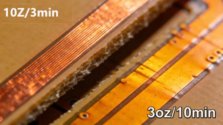
2.1.1 Copper Weight (Thickness): Supporting Current Requirements and Thermal Dissipation
Copper weight is typically measured in ounces (oz), with 1 oz of copper corresponding to a thickness of approximately 35μm (1.38 mils). The copper weight requirements for HMI PCBA vary between inner and outer layers, depending on the current load and thermal dissipation needs.
· Inner Layer Copper Weight: 0.5oz–2oz: The inner layers of HMI PCBA are primarily used for signal routing and ground/power planes, with lower current loads compared to the outer layers. For most HMI devices, a copper weight of 0.5oz to 2oz is sufficient to support signal transmission and provide adequate thermal dissipation. For consumer HMI PCBA with low-power components, 0.5oz to 1oz of copper is typically used to minimize cost and PCB thickness. For industrial/automotive HMI PCBA with higher current loads, 1oz to 2oz of copper is preferred to improve current-carrying capacity and thermal dissipation, reducing the risk of overheating in dense component layouts.
· Outer Layer Copper Weight: 1oz–3oz: The outer layers of HMI PCBA are exposed to the environment and support surface-mount components, power terminals, and connectors—all of which may carry higher currents. As such, the outer layers require thicker copper to handle higher current loads and provide better thermal dissipation. For consumer HMI PCBA, 1oz to 2oz of copper is sufficient to support the current requirements of backlight modules and touch ICs. For industrial/automotive HMI PCBA with high-current circuits (such as power supplies for large displays and control modules), 2oz to 3oz of copper is mandatory. This thicker copper not only supports higher current loads but also provides better resistance to corrosion and wear, which is critical for devices operating in harsh environments.
2.1.2 Trace Width and Spacing: Balancing Current Capacity and Miniaturization
Trace width and spacing are critical parameters for HMI PCBA, as they determine the current-carrying capacity of the traces, the level of crosstalk between adjacent traces, and the overall miniaturization of the PCB.
· 3mil/3mil Minimum Trace Width/Spacing for Consumer HMI PCBA: For miniaturized consumer HMI devices such as smartphones and smartwatches, fine-pitch traces are essential to accommodate dense component layouts. A minimum trace width and spacing of 3mil/3mil (0.076mm/0.076mm) is the industry standard for these devices, allowing for the routing of signals between 01005 SMD components and micro-SMD components in a compact space. It is important to note that 3mil traces have lower current-carrying capacity (approximately 0.1A for a 1oz copper trace) and are more susceptible to crosstalk—this is typically mitigated by using dedicated ground planes and signal isolation in consumer HMI PCBA design.
· 5mil/5mil Minimum Trace Width/Spacing for Industrial/Automotive HMI PCBA: For industrial and automotive HMI devices with high-current circuits (such as backlight modules and power supplies), wider traces and larger spacing are required to support higher current loads and reduce crosstalk. A minimum trace width and spacing of 5mil/5mil (0.127mm/0.127mm) is the industry standard for these devices, with 10mil/10mil traces used for high-current circuits (carrying 1A or more). Wider traces (5mil or more) have a higher current-carrying capacity (approximately 0.3A for a 1oz copper trace) and better thermal dissipation, reducing the risk of overheating and trace failure. Larger spacing between traces also reduces the risk of electrical arcing and crosstalk, which is critical for maintaining signal integrity in harsh electromagnetic environments.
2.1.3 Pad Size: Supporting Miniaturized and High-Pin-Count Components
Pads are the conductive areas on the PCB where components are soldered, and their size directly impacts the reliability of the solder joint and the ability to support miniaturized components. For HMI PCBA, the minimum pad size is determined by the type of components used.
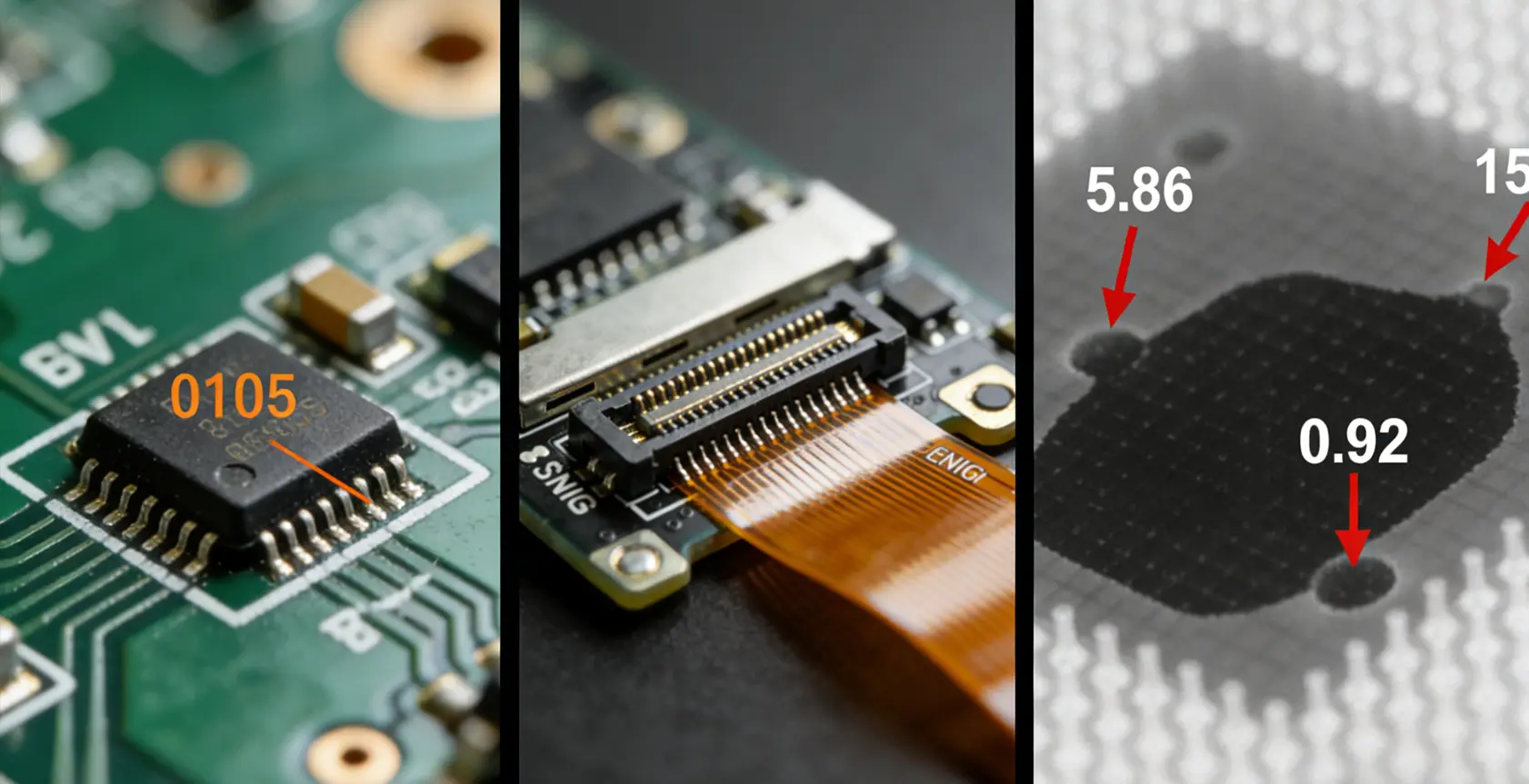
· Minimum 0.2mm Diameter Pads for Micro-SMD Components: For miniaturized SMD components such as 01005 and 0201, a minimum pad diameter of 0.2mm is required to ensure a reliable solder joint. These small pads are essential for miniaturized consumer HMI devices, where every millimeter of PCB space is critical. It is important to note that small pads require high SMD placement accuracy (±0.05mm for 0201 components) to ensure proper alignment during soldering, which can increase manufacturing costs and require advanced SMT equipment.
· Larger Pads for BGA/CSP Packages: For high-pin-count components such as BGA (ball grid array) packages for HMI processors and CSP (chip scale package) for touch ICs, larger pads (or solder balls) are required to support the high pin count and provide a reliable solder joint. BGA packages typically have a pad pitch of 0.4mm to 1.0mm, with solder balls that are soldered to the PCB using reflow soldering. These larger pads provide better mechanical stability and thermal dissipation, which is critical for high-performance industrial and automotive HMI devices.
2.2 Application-Specific Considerations for Copper Thickness and Traces
2.2.1 Consumer HMI PCBA: Fine-Pitch Traces and Miniaturization
For consumer HMI devices, the primary goals are miniaturization and cost control, which drives the use of fine-pitch traces (3mil/3mil) and thin copper (0.5oz–1oz inner layers, 1oz–2oz outer layers). Manufacturers must prioritize SMD placement accuracy to ensure reliable solder joints for miniaturized components, and they may use AOI (automated optical inspection) 100% for SMD components to detect and correct any placement or soldering defects. It is also important to use dedicated ground planes to reduce crosstalk and improve signal integrity in fine-pitch trace layouts.
2.2.2 Industrial/Automotive HMI PCBA: High-Current Traces and Thermal Dissipation
For industrial and automotive HMI devices, the primary goals are high current capacity and thermal dissipation, which drives the use of wider traces (5mil/5mil or larger) and thicker copper (1oz–2oz inner layers, 2oz–3oz outer layers). Manufacturers may also use copper pour for ground/power planes to improve thermal dissipation and current-carrying capacity, and they may implement impedance control (50Ω/100Ω) for touch signal lines to ensure signal integrity. Additionally, X-ray inspection for BGA/CSP void detection is used to detect any hidden solder defects in high-pin-count components, ensuring the reliability of the solder joint.
2.2.3 High-Frequency HMI PCBA: Impedance Control and Signal Integrity
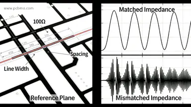
For HMI devices with high-frequency touch signal transmission (such as capacitive touchscreens with multi-touch functionality), impedance control is critical to maintaining signal integrity. Impedance is the total opposition to the flow of alternating current (AC) in a circuit, and it must be matched to the characteristic impedance of the touch panel and touch IC to avoid signal reflection and distortion. The standard impedance values for HMI touch signal lines are 50Ω for single-ended touch signals and 100Ω for differential touch signals. To achieve accurate impedance control, manufacturers must carefully control the copper thickness, trace width, spacing, and dielectric thickness of the PCB substrate—this is where Rogers 4350B shines, as its low and stable dielectric constant allows for precise impedance control at high frequencies.
3. Surface Finish: Protecting Conductive Surfaces and Ensuring Solderability
The surface finish of an HMI PCBA is a thin protective layer applied to the copper traces and pads to prevent oxidation, improve solderability, and enhance corrosion resistance. Choosing the right surface finish is critical to ensuring reliable solder joints, long-term performance, and cost-effectiveness—particularly in harsh environments where the HMI device may be exposed to moisture, chemicals, and extreme temperatures. This section explores the core technical parameters for HMI PCBA surface finish options, including ENIG (electroless nickel immersion gold), OSP (organic solderability preservative), and immersion silver/tin, with a focus on application-specific considerations for consumer, industrial, and automotive HMI.
3.1 Core Technical Specifications for HMI PCBA Surface Finishes
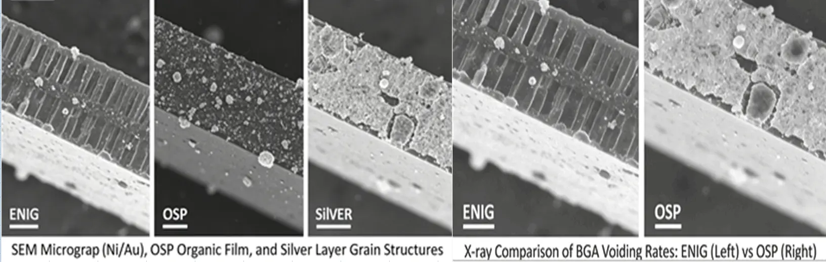
3.1.1 ENIG (Electroless Nickel Immersion Gold): High Reliability for Harsh Environments
ENIG is a premium surface finish that consists of a layer of nickel (3–5μm) deposited on the copper surface, followed by a thin layer of gold (0.05–0.1μm) deposited on the nickel layer. The nickel layer acts as a barrier between the copper and gold, preventing diffusion and oxidation, while the gold layer provides excellent solderability, corrosion resistance, and electrical conductivity.
Key technical specifications for ENIG:
· Nickel Thickness: 3–5μm (strikes the balance between barrier protection and solderability)
· Gold Thickness: 0.05–0.1μm (sufficient for most HMI applications; thicker layers for extreme harsh environments)
ENIG is known for its excellent flatness, making it ideal for BGA packages for HMI processors and FPC (flexible printed circuit) connectors (0.3mm/0.5mm pitch)—both requiring a flat, reliable surface for soldering. It also has an excellent long-term shelf life (up to 12 months) without oxidation, critical for manufacturers who may store PCBs before assembly.
3.1.2 OSP (Organic Solderability Preservative): Cost-Effective for Consumer HMI
OSP is a cost-effective surface finish that consists of a thin organic layer (0.2–0.5μm) deposited on the copper surface to prevent oxidation. Unlike ENIG, OSP does not contain any metal layers—it relies on the organic film to protect the copper from oxidation and improve solderability.
Key technical specifications for OSP:
· OSP Thickness: 0.2–0.5μm (provides adequate protection for up to 6 months of shelf life in dry, cool storage)
· Solderability: Excellent for reflow soldering (primary soldering method for SMD components on HMI PCBA)
OSP is the most cost-effective surface finish option for HMI PCBA, making it ideal for consumer HMI PCBA where cost control is a top priority. However, it has limitations: less durable than ENIG, susceptible to damage from moisture and handling, shorter shelf life, and not suitable for wave soldering or devices requiring multiple reflow cycles.
3.1.3 Immersion Silver/Tin: Balancing Performance and Cost
Immersion silver and immersion tin are mid-range surface finishes that offer a balance between performance and cost, suitable for a wide range of HMI applications.
Key technical specifications:
· Immersion Silver Thickness: 0.5–1.0μm (excellent solderability and corrosion resistance; shelf life up to 9 months)
· Immersion Tin Thickness: 0.5–1.0μm (excellent solderability and wear resistance; shelf life up to 12 months)
Immersion silver/tin offers better durability and shelf life than OSP, and it is more cost-effective than ENIG. It is suitable for both reflow and wave soldering, making it ideal for HMI PCBA that includes both SMD and through-hole components (such as connectors and power terminals for industrial HMI). However, immersion silver is susceptible to tarnishing in sulfur-containing environments, and immersion tin can form a brittle intermetallic layer with copper if exposed to high temperatures for prolonged periods.
3.2 Application-Specific Considerations for HMI PCBA Surface Finishes
3.2.1 Consumer HMI PCBA: Cost-Effective OSP for Mass Production
For consumer HMI devices, cost control is a top priority, making OSP surface finish the optimal choice. OSP provides sufficient protection and solderability for normal operating conditions, and it is significantly less expensive than ENIG or immersion silver/tin. Manufacturers can further optimize costs by using OSP in combination with reflow soldering and AOI inspection to ensure high yield rates. It is important to store OSP-coated PCBs in a dry, cool environment to prevent oxidation and extend shelf life.
3.2.2 Industrial/Automotive HMI PCBA: ENIG for High Reliability
For industrial and automotive HMI devices operating in harsh environments, ENIG surface finish is the gold standard. ENIG provides excellent corrosion resistance, solderability, and durability, ensuring long-term performance in extreme temperatures, high humidity, and corrosive environments. It is also ideal for BGA packages and FPC connectors, which require a flat, reliable surface for soldering. While ENIG is more expensive than OSP or immersion silver/tin, the added reliability is well worth the cost for mission-critical industrial and automotive HMI devices.
3.2.3 Mid-Range HMI PCBA: Immersion Silver/Tin for Balanced Performance
For mid-range HMI devices that require a balance between performance and cost, immersion silver/tin surface finish is an excellent choice. It offers better durability and shelf life than OSP, and it is more cost-effective than ENIG. It is suitable for a wide range of HMI applications, including commercial equipment and mid-range industrial devices, and it can accommodate both SMD and through-hole components.
4. Component Assembly Specifications: Precision and Compatibility for HMI Functionality
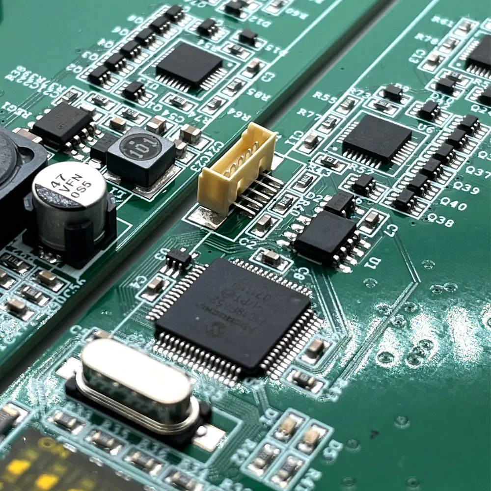
Component assembly is the process of mounting and soldering components onto the HMI PCB, and it is one of the most critical stages in HMI PCBA manufacturing. The precision of component placement, the compatibility of components with the PCB, and the quality of the solder joint all directly impact the functionality and reliability of the HMI device. As HMI devices become more miniaturized and high-performance, the requirements for SMT (surface mount technology) assembly for HMI PCBA and component compatibility have become increasingly stringent. This section explores the core technical parameters for HMI PCBA component assembly, including component types, SMT placement accuracy, and connector compatibility, with a focus on application-specific considerations for consumer, industrial, and automotive HMI.
4.1 Core Technical Specifications for HMI PCBA Component Assembly
4.1.1 Component Types: SMD for Miniaturization, Through-Hole for Ruggedness
HMI PCBA utilizes two primary types of components: surface-mount devices (SMDs) and through-hole components. Each type has unique advantages and is suitable for different application scenarios.
· SMD Components (01005 to QFP/BGA/CSP): SMD components are the dominant component type for HMI PCBA, thanks to their small size, high component density, and compatibility with automated assembly processes. The range of SMD components used in HMI PCBA includes:
o 01005/0201 SMD Components: The smallest SMD components, used for miniaturized consumer HMI devices such as smartwatches and fitness trackers. These require high SMD placement accuracy and advanced SMT equipment for assembly.
o 0402/0603/0805 SMD Components: The most commonly used SMD components, suitable for a wide range of HMI devices (consumer, industrial, automotive) for passive components (resistors, capacitors, inductors) and small active components (diodes, transistors).
o QFP (Quad Flat Package) Components: High-pin-count SMD components used for touch ICs and control modules in mid-range HMI devices.
o BGA/CSP Packages: High-performance SMD components used for HMI processors, high-resolution display drivers, and advanced touch ICs in industrial and automotive HMI devices. These offer high pin density and excellent thermal performance but require X-ray inspection to detect hidden solder defects.
· Through-Hole Components (Connectors, Power Terminals): Through-hole components are inserted through holes in the PCB and soldered on the opposite side, providing excellent mechanical stability and high current-carrying capacity. They are primarily used for connectors for HMI data transmission (HDMI, USB-C, RS232/485) and power terminals for high-current HMI circuits in industrial and automotive HMI devices. While less suitable for miniaturization, they offer superior ruggedness and resistance to vibration and shock—critical for devices operating in harsh environments.
4.1.2 SMT Placement Accuracy: Ensuring Reliable Solder Joints and Component Functionality
SMT placement accuracy is the measure of how precisely the SMT equipment can place components onto the PCB pads, and it is critical to ensuring reliable solder joints and component functionality.
· ±0.05mm placement accuracy for 0201 SMD components (ensures proper alignment with PCB pads; misalignment beyond this tolerance leads to poor solder joints or failure).
· ±0.03mm placement accuracy for BGA packages (pitch ≤0.5mm) (requires advanced SMT equipment with vision systems for high pin-count alignment).
· ±0.1mm placement accuracy for larger SMD components (0402 and above) (sufficient for reliable solder joints, cost-effective for mass production).
4.1.3 Connector Compatibility: Ensuring Seamless Data Transmission and Power Delivery
Connectors are critical components for HMI devices, enabling seamless data transmission and power delivery.
· FPC (Flexible Printed Circuit) Connectors (0.3mm/0.5mm Pitch): Widely used to connect the PCBA to flexible displays and touch panels. 0.3mm pitch connectors are for miniaturized consumer HMI devices, while 0.5mm pitch connectors are for industrial and automotive HMI devices. They require a flat, reliable surface finish (such as ENIG) and precise placement for secure connections.
· HDMI/USB-C Connectors for HMI Data Transmission: HDMI transmits high-resolution video and audio signals, while USB-C transmits data and power. These are typically through-hole components (for ruggedness) and must comply with industry standards (HDMI 2.1, USB 3.2) for compatibility. Commonly used in automotive infotainment systems, industrial control panels, and consumer HMI devices like tablets and smart TVs.
· RS232/RS485 Connectors for Industrial HMI Communication: Designed for long-distance data transmission (up to 1.2km for RS485) and resistance to electromagnetic interference. Ideal for factory automation and outdoor monitoring systems, they are typically through-hole components with rugged housing to withstand harsh industrial environments.
4.2 Application-Specific Considerations for HMI PCBA Component Assembly
4.2.1 Consumer HMI PCBA: Miniaturized SMD Components and Automated Assembly
For consumer HMI devices, the primary goals are miniaturization and mass production, driving the use of 01005/0201 SMD components and automated SMT assembly processes. Manufacturers must invest in advanced SMT equipment with high placement accuracy to ensure reliable solder joints, and they may use AOI (automated optical inspection) 100% for SMD components to detect and correct defects. FPC connectors (0.3mm pitch) are preferred for connecting to flexible displays and touch panels, meeting miniaturization requirements.
4.2.2 Industrial/Automotive HMI PCBA: Rugged Components and Rigorous Inspection
For industrial and automotive HMI devices, the primary goals are ruggedness and reliability, leading to the use of BGA/CSP packages (for high performance), through-hole components (for ruggedness), and rigorous inspection processes. Manufacturers must use X-ray inspection for BGA/CSP void detection, and may perform manual inspection for through-hole components. Additionally, conformal coating may be required to protect components from moisture, chemicals, and dust—enhancing reliability in harsh environments.
4.2.3 High-Performance HMI PCBA: BGA Packages and Signal Integrity
For high-performance HMI devices such as automotive infotainment systems and industrial control panels with high-resolution displays, BGA packages are essential to accommodate the high pin count of advanced processors and display drivers. These packages offer excellent thermal performance and signal integrity but require precise placement and soldering. Manufacturers must also prioritize impedance control for high-speed data lines (HDMI/USB-C) and may use EMI shielding to reduce electromagnetic interference.
5. Electrical Performance: Ensuring Signal Integrity and Reliable Operation
The electrical performance of an HMI PCBA is critical to ensuring reliable signal transmission, stable power delivery, and resistance to electromagnetic interference. Inadequate electrical performance can lead to touch signal distortion, display flicker, component failure, and erratic device operation—particularly in high-frequency and high-noise environments. This section explores the core technical parameters for HMI PCBA electrical performance, including dielectric constant, insulation resistance, withstand voltage, and touch signal line impedance, with a focus on application-specific considerations for consumer, industrial, and automotive HMI.
5.1 Core Technical Specifications for HMI PCBA Electrical Performance
5.1.1 Dielectric Constant (Dk): Ensuring Signal Integrity at High Frequencies
Dielectric constant (Dk) is the measure of a material’s ability to store electrical energy in an electric field, critical for high-frequency HMI PCBA. A low and stable Dk reduces signal attenuation, reflection, and crosstalk.
· FR-4 dielectric constant: 4.2–4.5 at 1GHz (sufficient for most consumer and low-frequency industrial HMI devices; Dk varies with temperature and frequency).
· Rogers 4350B dielectric constant: 3.48 at 1GHz (low and stable, ideal for high-frequency HMI devices like capacitive touchscreens; consistent performance across temperature and frequency ranges).
5.1.2 Insulation Resistance: Preventing Signal Leakage and Interference
Insulation resistance is the measure of a material’s ability to resist electrical current through its insulating layers, critical for preventing signal leakage and interference between adjacent traces. The minimum requirement for HMI PCBA is ≥10¹⁰Ω at 500V DC, ensuring current remains confined to intended traces.
5.1.3 Withstand Voltage: Resisting Electrical Arcing and Breakdown
Withstand voltage (dielectric strength) is the measure of a material’s ability to resist electrical arcing and breakdown between adjacent traces or components. The minimum requirement for HMI PCBA is AC 1.5kV for 1min (between adjacent traces), withstanding transient voltage spikes (ESD, power surges) to avoid short circuits and component failure.
5.1.4 Touch Signal Line Impedance: Ensuring Accurate Touch Detection
Touch signal line impedance control (50Ω/100Ω) is critical for stable touch signal transmission in capacitive HMI devices. 50Ω is used for single-ended touch signals, while 100Ω is for differential touch signals. Precise impedance control ensures accurate and rapid touch detection, even in noisy electromagnetic environments.
5.2 Application-Specific Considerations for HMI PCBA Electrical Performance
For consumer HMI devices, electrical performance requirements are relatively moderate—FR-4 substrate and standard impedance control suffice for normal operation. For industrial and automotive HMI devices, stringent requirements are mandatory: low and stable Dk (Rogers 4350B), high insulation resistance (≥10¹⁰Ω), and high withstand voltage (AC 1.5KV for 1min). Additionally, industrial HMI devices may require EMI filtering components to reduce interference from other industrial equipment, ensuring reliable operation in high-noise environments.
6. Thermal & Environmental Performance: Ruggedness for Harsh Operating Conditions
HMI devices often operate in harsh environments characterized by extreme temperatures, high humidity, heavy vibration, and exposure to moisture and chemicals. As such, the thermal and environmental performance of the HMI PCBA is critical to ensuring long-term reliability and functionality. This section explores the core technical parameters for HMI PCBA thermal & environmental performance, including operating temperature range, thermal expansion coefficient (CTE), and humidity resistance, with a focus on application-specific considerations for consumer, industrial, and automotive HMI.
6.1 Core Technical Specifications for HMI PCBA Thermal & Environmental Performance
6.1.1 Operating Temperature Range: Adapting to Extreme Environments
The operating temperature range of an HMI PCBA is the range of temperatures within which the device can operate reliably without performance degradation or component failure.
· Consumer HMI PCBA operating temperature: 0°C to 60°C (sufficient for indoor environments with moderate temperatures, covering smartphones, tablets, and smart home control panels).
· Industrial/automotive HMI PCBA operating temperature: -40°C to 85°C (mandatory for harsh environments with extreme temperature fluctuations, covering outdoor industrial settings and automotive engine compartments).
6.1.2 Thermal Expansion Coefficient (CTE): Preventing Warpage and Solder Joint Cracking
CTE is the measure of a material’s tendency to expand or contract with temperature changes, critical for preventing warpage and solder joint cracking.
· X/Y-axis CTE: 12–18 ppm/°C (low, ensuring the PCB maintains dimensional integrity with temperature changes, reducing trace cracking and component misalignment).
· Z-axis CTE: 60–80 ppm/°C (higher, potentially leading to delamination and solder joint cracking under thermal cycling; mitigated by high-Tg substrates and underfill materials for BGA packages).
6.1.3 Humidity Resistance: Withstanding Moisture and Condensation
Humidity resistance is the measure of a material’s ability to withstand high humidity without performance degradation or component failure. The minimum requirement for HMI PCBA is passing 85°C/85% RH for 1000hrs (no functional failure), simulating prolonged exposure to high humidity (industrial workshops, tropical environments) to avoid corrosion, delamination, or short circuits.
6.2 Application-Specific Considerations for HMI PCBA Thermal & Environmental Performance
For consumer HMI devices, thermal and environmental performance requirements are relatively moderate—a standard operating temperature range (0°C to 60°C) and humidity resistance suffice for normal indoor operation. For industrial and automotive HMI devices, stringent requirements are mandatory: wide operating temperature range (-40°C to 85°C), low Z-axis CTE, and high humidity resistance (85°C/85% RH for 1000hrs). Additionally, industrial and automotive HMI PCBA may require conformal coating (acrylic or urethane) to protect components from moisture, chemicals, and dust, further enhancing reliability in harsh environments.
7. Reliability & Test Standards: Ensuring Consistent Quality and Performance
Reliability testing is the process of evaluating the HMI PCBA’s ability to withstand the stresses of normal operation and harsh environments, ensuring consistent quality and performance over its lifespan. Compliance with industry standards and rigorous testing protocols is non-negotiable for high-reliability HMI applications, particularly in industrial and automotive sectors where failure can lead to safety risks or significant downtime.
7.1 Key Reliability Test Standards for HMI PCBA
· IPC Class 3 Compliance: The highest standard for PCB reliability, required for industrial and automotive HMI PCBA. It mandates strict quality control for solder joints, trace integrity, and component placement, ensuring resistance to environmental stressors and long-term stability.
· AEC-Q100 (Automotive Electronics Council): A critical standard for automotive HMI PCBA components (integrated circuits, SMDs). It includes rigorous testing for temperature cycling, humidity, vibration, and electrical stress, ensuring components can withstand the harsh automotive environment.
· IEC 60068-2-6 (Vibration Test): Mandatory for industrial and automotive HMI PCBA, this test evaluates the PCB’s resistance to mechanical vibration (simulating factory floors or vehicle operation) to prevent component detachment or trace damage.
· 85°C/85% RH Humidity Resistance Test (1000hrs): As noted in Section 6, this test ensures HMI PCBA can withstand prolonged high humidity without functional failure, critical for industrial and outdoor HMI applications.
· Thermal Cycling Test: Evaluates the PCB’s ability to withstand extreme temperature fluctuations (-40°C to 85°C for automotive, 0°C to 85°C for industrial), preventing warpage, delamination, and solder joint cracking.
7.2 Application-Specific Reliability Considerations
For consumer HMI PCBA, reliability testing focuses on basic functionality and durability under normal use (temperature range 0°C to 60°C, standard humidity resistance). Compliance with IPC Class 2 (general electronics standard) is typically sufficient, balancing cost and performance.
For industrial and automotive HMI PCBA, reliability testing is far more rigorous. Compliance with IPC Class 3, AEC-Q100 (automotive), and IEC 60068 standards is mandatory. Additional tests may include ESD (electrostatic discharge) testing (IEC 61000-4-2) to protect against static damage, and chemical resistance testing (for exposure to oils, coolants, or industrial chemicals) to ensure long-term functionality in harsh environments.
· Substrate Material: FR-4 (Tg ≥ 130°C/170°C for industrial HMI), Aluminum PCB (for high-heat HMI backplanes), Rogers 4350B (for high-frequency touch signal transmission)
· PCB Layers: 2–12 layers (2–4 layers for consumer HMI; 6–12 layers for industrial/automotive HMI with integrated control modules)
· Board Thickness: 0.4mm–2.0mm (standard: 1.0mm/1.6mm)
· Copper Weight: Inner Layer: 0.5oz–2oz; Outer Layer: 1oz–3oz
· Trace Width/Spacing: Min. 3mil/3mil (consumer HMI); Min. 5mil/5mil (industrial HMI for high-current circuits)
· Pad Size: Min. 0.2mm diameter (for micro-SMD components)
· ENIG (Electroless Nickel Immersion Gold): 3–5μm nickel, 0.05–0.1μm gold
· OSP (Organic Solderability Preservative): 0.2–0.5μm thickness
· Immersion Silver/Tin: 0.5–1.0μm thickness
· Component Type: SMD (01005 to QFP/BGA/CSP), Through-Hole (connectors, power terminals)
· SMT Placement Accuracy: ±0.05mm for 0201 components; ±0.03mm for BGA (pitch ≤0.5mm)
· Connector Compatibility: FPC (0.3mm/0.5mm pitch), HDMI, USB-C, RS232/485 (for HMI data transmission)
· Dielectric Constant (Dk): 4.2–4.5 (FR-4 at 1GHz); 3.48 (Rogers 4350B)
· Insulation Resistance: ≥10¹⁰Ω at 500V DC
· Withstand Voltage: AC 1.5kV for 1min (between adjacent traces)
· Touch Signal Line Impedance: 50Ω/100Ω (matched for capacitive touch panels)
· Operating Temperature Range: Consumer HMI: 0°C to 60°C; Industrial/Automotive HMI: -40°C to 85°C
· Thermal Expansion Coefficient (CTE): X/Y: 12–18 ppm/°C; Z-axis: 60–80 ppm/°C
· Humidity Resistance: Passes 85°C/85% RH for 1000hrs (no functional failure)
· IPC Standards Compliance: IPC-A-610 (Class 2 for consumer; Class 3 for industrial/automotive)
· Temperature Cycling Test: -40°C to 85°C, 1000 cycles (no solder joint defects)
· Vibration Test: 5–2000Hz, 10G acceleration (meets IEC 60068-2-6)
· Inspection: AOI (100% for SMD components), X-Ray (for BGA/CSP void detection)
· ITO Coating Resistance (for capacitive HMI): 100–500Ω/sq (uniformity ±10%)
· Backlight Driver Circuit Tolerance: ±2% current accuracy
· ESD Protection: ±8kV (contact), ±15kV (air) (complies with IEC 61000-4-2)
1. All parameters are customizable based on HMI application scenarios (consumer, industrial, automotive, medical).
2. Compliance with industry standards (IPC, IEC, ISO) is mandatory for high-reliability HMI products.
3. Impedance control and signal integrity simulation are recommended for HMI with high-resolution touch displays.