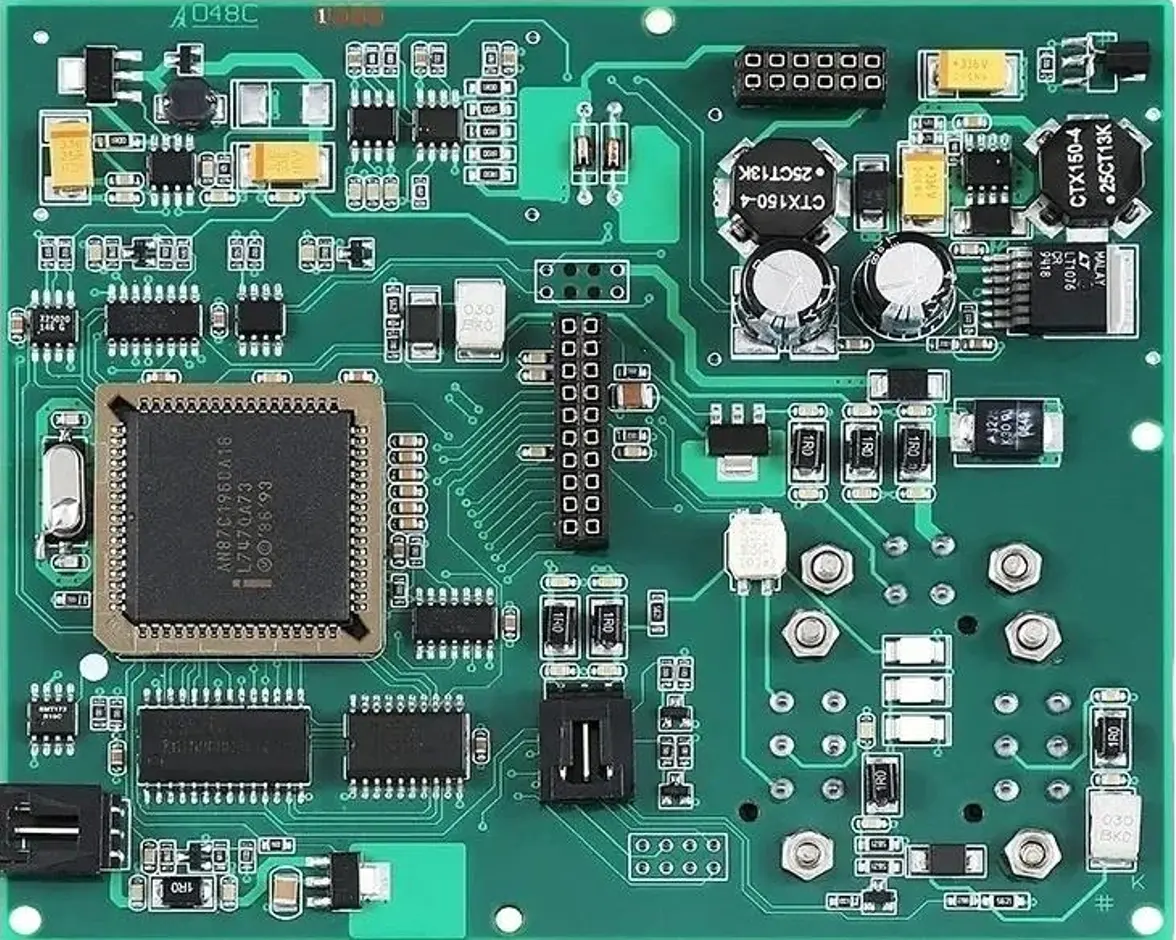
DC/DC converter printed circuit board assemblies (PCBAs) are the backbone of modern power electronics, enabling efficient voltage conversion across industries ranging from automotive and aerospace to consumer electronics and industrial automation. As the demand for compact, high‑performance, and reliable power solutions grows, the manufacturing of DC/DC converter PCBAs demands rigorous adherence to technical specifications and industry best practices. This article explores the critical manufacturing parameters, material selection, and quality standards that define high‑performance DC/DC converter PCBAs.
The foundation of a reliable DC/DC converter PCBA lies in substrate material selection, which directly impacts thermal stability, electrical performance, and durability.
Standard Material: FR‑4 remains the industry benchmark for standard applications, offering a balance of cost‑effectiveness and mechanical strength.
High‑Temperature Environments: High‑TG FR‑4 (≥170°C) resists deformation under thermal stress.
High‑Frequency Converters: For applications such as RF power systems, advanced materials like Rogers 4350B/RO4003C or Arlon AD255C are preferred—these substrates minimize signal loss and maintain consistent impedance at high frequencies.
Physical Specifications:
PCB Thickness: Tailored to design requirements—ranges from 0.4 mm (compact consumer devices) to 2.0 mm (heavy‑duty industrial converters).
Layer Count:
2‑layer boards: Suffice for basic low‑power converters.
Up to 12 layers: Support complex power distribution and signal isolation in aerospace and medical applications.
Copper Thickness:
1 oz (35 μm): Suits low‑current applications.
2 oz (70 μm) or 3 oz (105 μm): Mandatory for high‑current converters (up to 50 A).
Plated through‑hole copper thickness: ≥20 μm—ensuring reliable connectivity.
To maintain electrical performance, DC/DC converter PCBAs require tight tolerances for trace geometry and via design.
Trace Geometry:
Minimum line width/spacing: 3 mil (0.076 mm) —standard.
Fine‑pitch designs: Down to 2 mil/2 mil for high‑density layouts—prevents signal crosstalk and ensures stable power delivery.
Via Specifications:
Mechanical vias: Minimum 0.3 mm hole / 0.6 mm pad—used for standard connections.
Blind/Buried vias: 0.15 mm hole / 0.35 mm pad—optimize space in multi‑layer boards.
Filled vias: Epoxy or conductive resin fill—enhance thermal conductivity and prevent solder wicking in power‑dense areas.
Solder Mask and Silkscreen:
Liquid Photoimageable Solder Mask (LPI): Minimum 2 mil bridge ensures robust insulation. Color options (green, black, white, red) meet industry or branding requirements.
Silkscreen Printing: 1200+ DPI resolution, 0.8 mm minimum character height—enables clear component labeling and traceability, critical for assembly and maintenance.
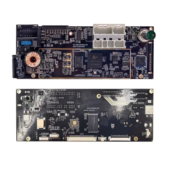
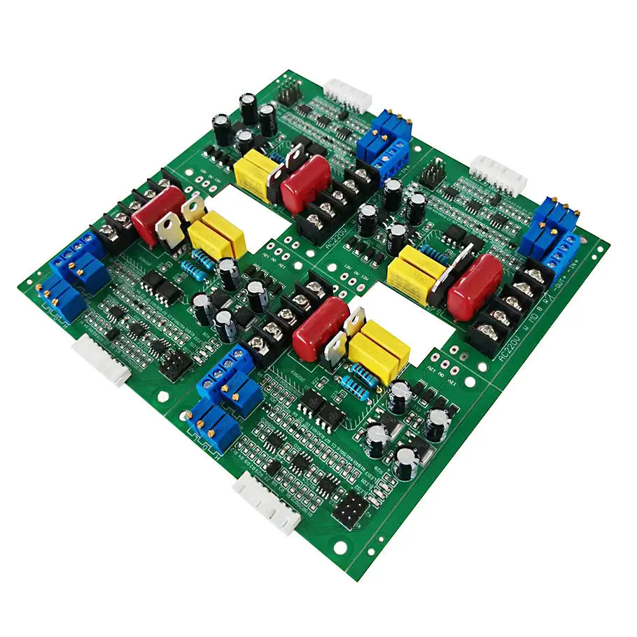
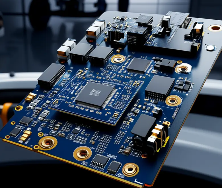
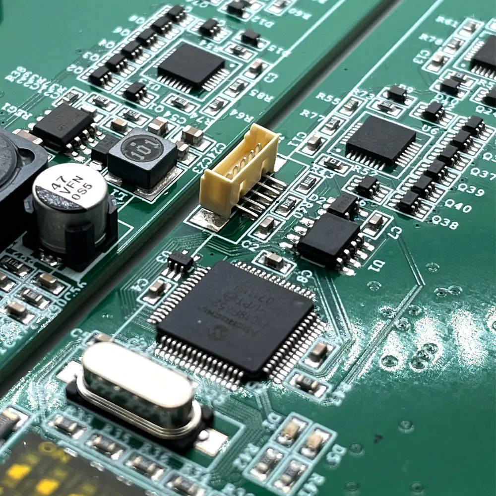
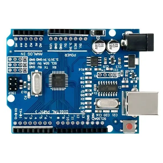
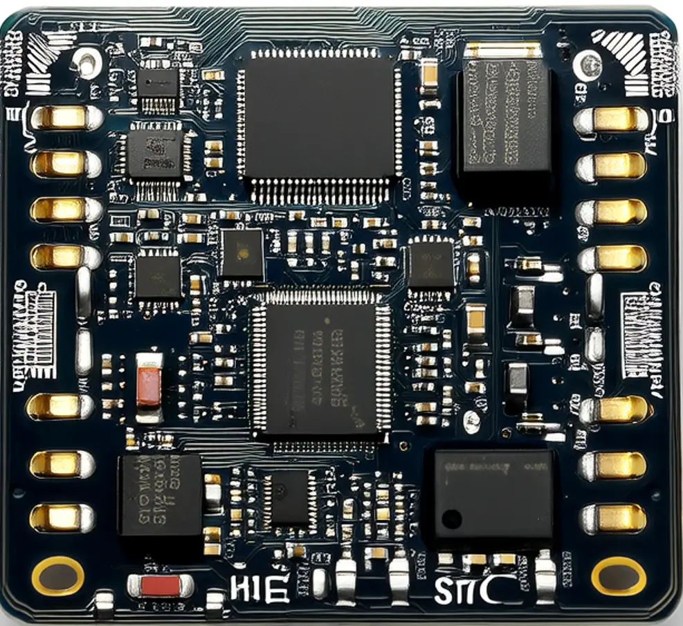
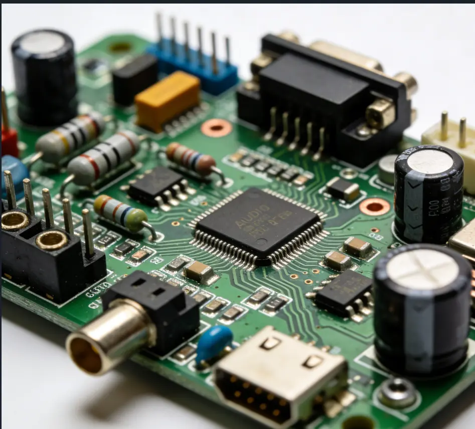
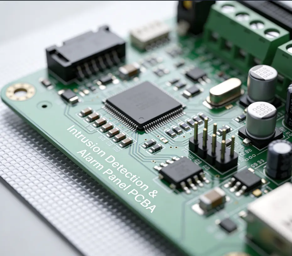
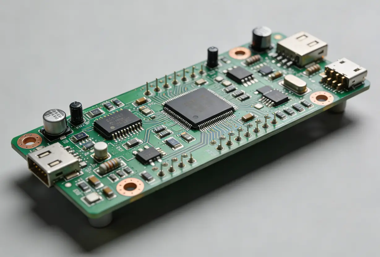
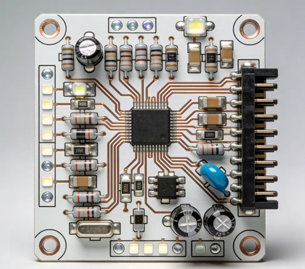
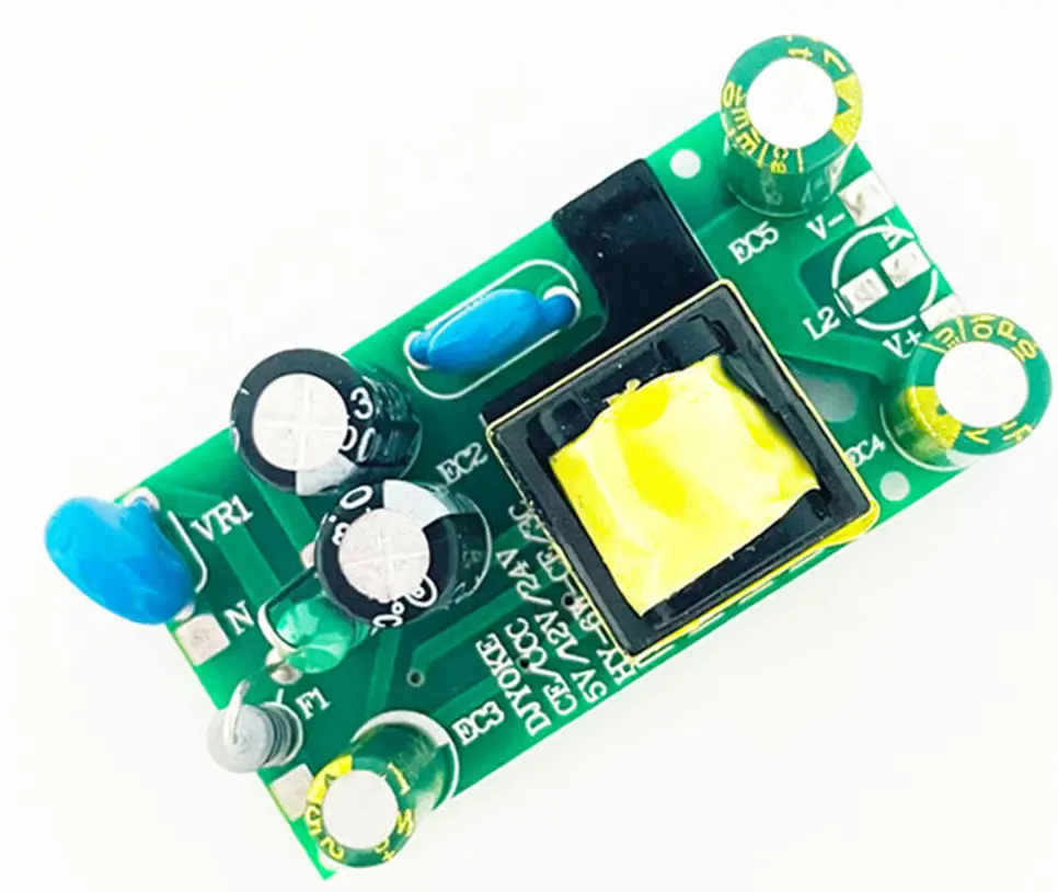
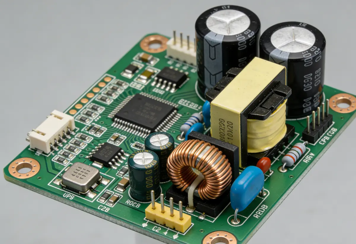
DC/DC converter PCBAs integrate both surface‑mount technology (SMT) and through‑hole technology (THT) components to balance miniaturization and mechanical strength.
SMT Components:
Ultra‑small form factors: 01005, 0201—for compact designs.
High‑power packages: QFP, QFN, BGA—for power ICs.
THT Components: Axial, radial, DIP—used for high‑voltage or high‑vibration applications where mechanical stability is paramount.
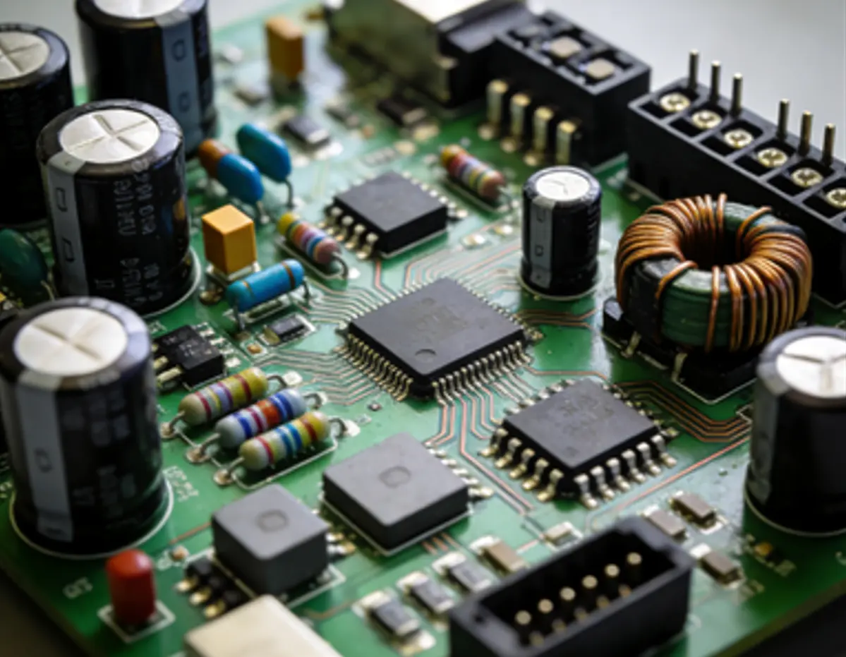
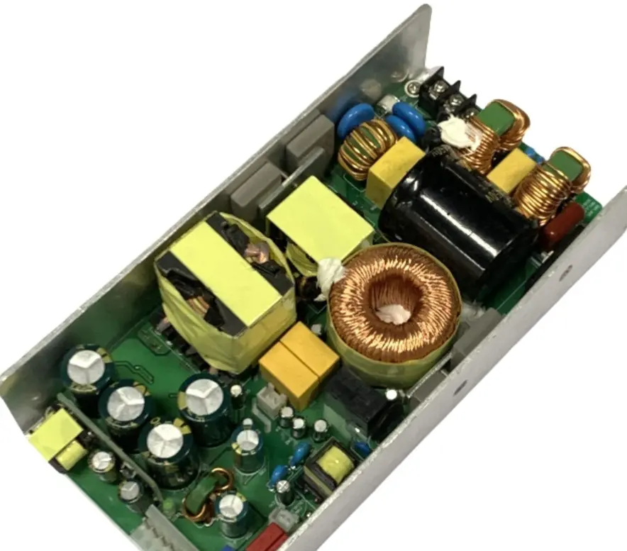
Soldering and Thermal Management:
Lead‑free Soldering: SAC305 alloy (Sn96.5/Ag3.0/Cu0.5) —mandatory for RoHS compliance.
Reflow Soldering Profile: Peaks at 245°C ±5°C—ensures strong solder joints.
Thermal Pads: Power ICs require ≥80% coverage to dissipate heat effectively.
Thermal Relief Pads: On high‑power vias—prevent heat buildup and solder cracking.
Heat Sink Compatibility: Mechanical fastening or adhesive mounting—enhances thermal performance in high‑power converters.
Reliable DC/DC converter PCBAs must meet stringent electrical and environmental standards.
Electrical Safety:
Isolation Resistance: ≥10¹⁰ Ω (at 500V DC).
Dielectric Withstand Voltage: 2.5 kV AC for 1 min (for reinforced isolation)—ensuring safety in high‑voltage applications.
Impedance Control: 50 Ω, 75 Ω, 100 Ω characteristic impedance; 90 Ω / 100 Ω differential impedance—±10% tolerance—maintains signal integrity in high‑frequency converters.
Environmental Compliance:
RoHS 2 and REACH.
IPC‑A‑610 Class 2 (commercial) or Class 3 (aerospace/medical)—governing assembly quality.
Comprehensive Testing Validates Performance:
In‑Circuit Test (ICT): Verifies 100% of solder joints and component connectivity.
Functional Test (FCT): Validates output voltage accuracy, load regulation, ripple/noise, and efficiency.
Thermal Cycling: -40°C to +125°C for 1000 cycles—tests thermal durability.
Burn‑In Test: 12–24 hours at rated load/temperature—identifies early‑life failures.
DC/DC converter PCBAs are engineered to deliver precision, efficiency, and reliability in the most demanding power applications. From substrate material selection to post‑manufacturing testing, every parameter—copper thickness, via design, thermal management, and compliance—plays a critical role in performance. By adhering to the technical specifications outlined here, manufacturers can produce PCBAs that meet the rigorous demands of modern power electronics, ensuring long‑term functionality across automotive, industrial, aerospace, and consumer markets. As power conversion technology evolves, the focus on precision manufacturing and thermal optimization will remain central to advancing DC/DC converter PCBA performance.
|
Parameter Category |
Technical Specifications |
|
Substrate Material |
FR-4 (Standard), High TG FR-4 (≥170°C), |
|
PCB Thickness |
0.4mm – 2.0mm, Customizable per Design Requirements |
|
Number of Layers |
2-layer, 4-layer, 6-layer, 8-layer (Up to 12-layer for High-Density Designs) |
|
Copper Thickness |
1oz (35μm), 2oz (70μm), 3oz (105μm) – Inner/Outer Layers; |
|
Minimum Line Width & Spacing |
Line Width: 3mil (0.076mm); |
|
Via Specifications |
- Mechanical Via: Minimum Diameter 0.3mm (Hole) / 0.6mm (Pad) |
|
Solder Mask |
Green (Standard), Black, White, Red; |
|
Silkscreen |
White/Black Ink; Minimum Character Height 0.8mm; |
|
Component Assembly |
- SMT Components: 01005, 0201, 0402, 0603, 0805, |
|
Solder Paste & Soldering |
Lead-Free Solder Paste (SAC305: Sn96.5/Ag3.0/Cu0.5); |
|
Thermal Management |
- Thermal Pad Design for Power ICs (≥80% Coverage) |
|
Voltage & Current Rating |
- Operating Voltage: Up to 600V DC |
|
Isolation Resistance |
≥10¹⁰ Ω at 500V DC (Between Input/Output, |
|
Dielectric Withstand Voltage |
2.5kV AC (1min) for Reinforced Isolation; |
|
Impedance Control |
Characteristic Impedance: 50Ω, 75Ω, 100Ω (±10% Tolerance); |
|
Environmental Compliance |
RoHS 2 (Directive 2011/65/EU), REACH, |
|
Testing Standards |
- In-Circuit Test (ICT): 100% Coverage of Solder Joints & Component Connectivity |