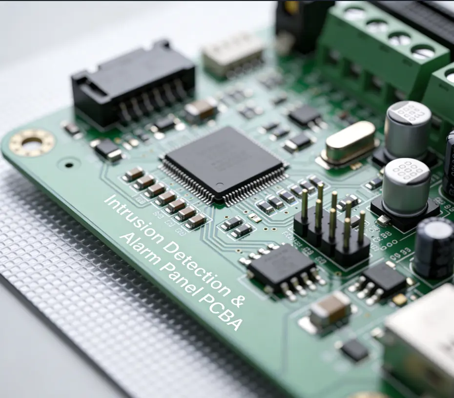
Base Station & RRU/AAU PCBA: Core Technologies for 5G Connectivity
Printed Circuit Board Assemblies (PCBAs) are the backbone of base stations, Remote Radio Units (RRUs), and Active Antenna Units (AAUs)—the critical infrastructure powering 5G networks. As 5G deployments scale globally, base station and RRU/AAU PCBA design, material selection, and manufacturing processes have become pivotal to achieving ultra-low latency, high bandwidth, and massive device connectivity. This article explores the technical nuances, key challenges, and innovative solutions of base station & RRU/AAU PCBA.
RRU vs. AAU: PCB Assembly Differences and Applications
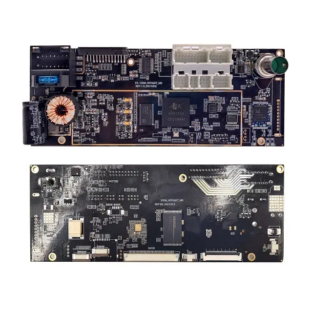
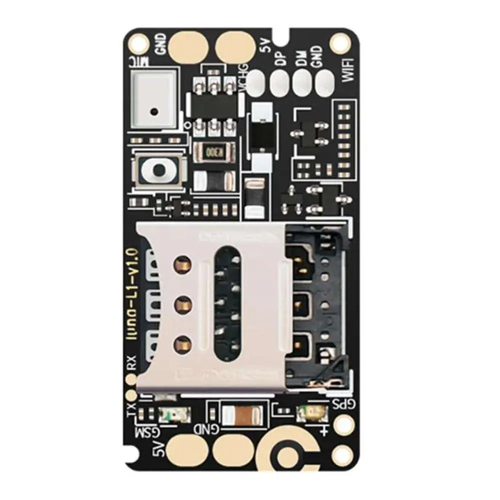
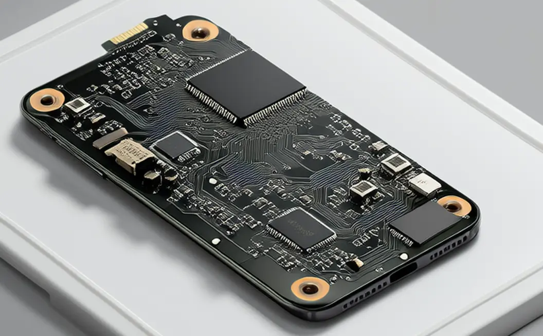
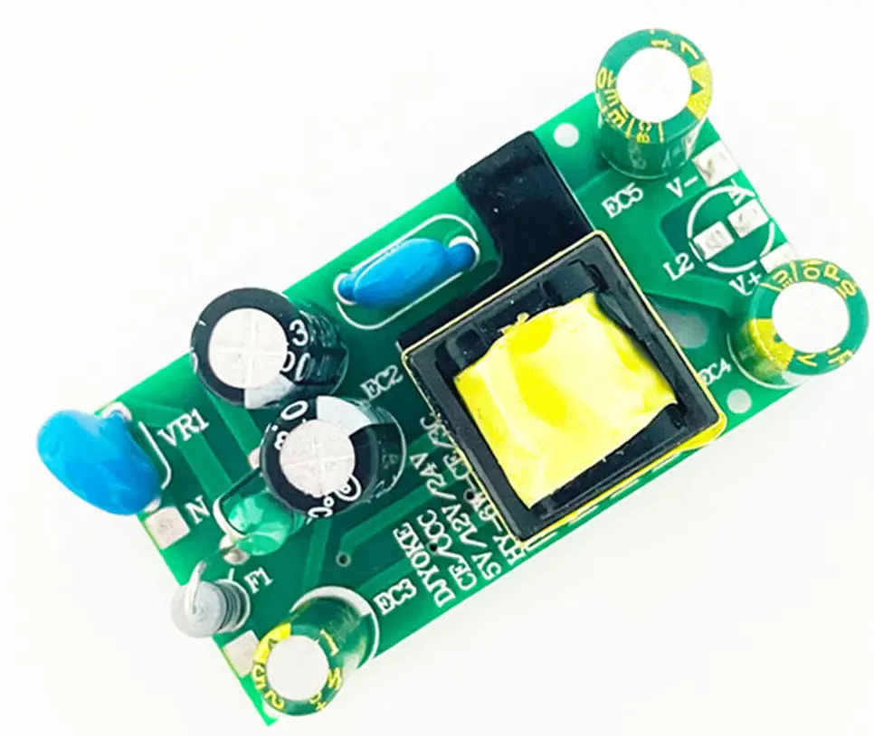
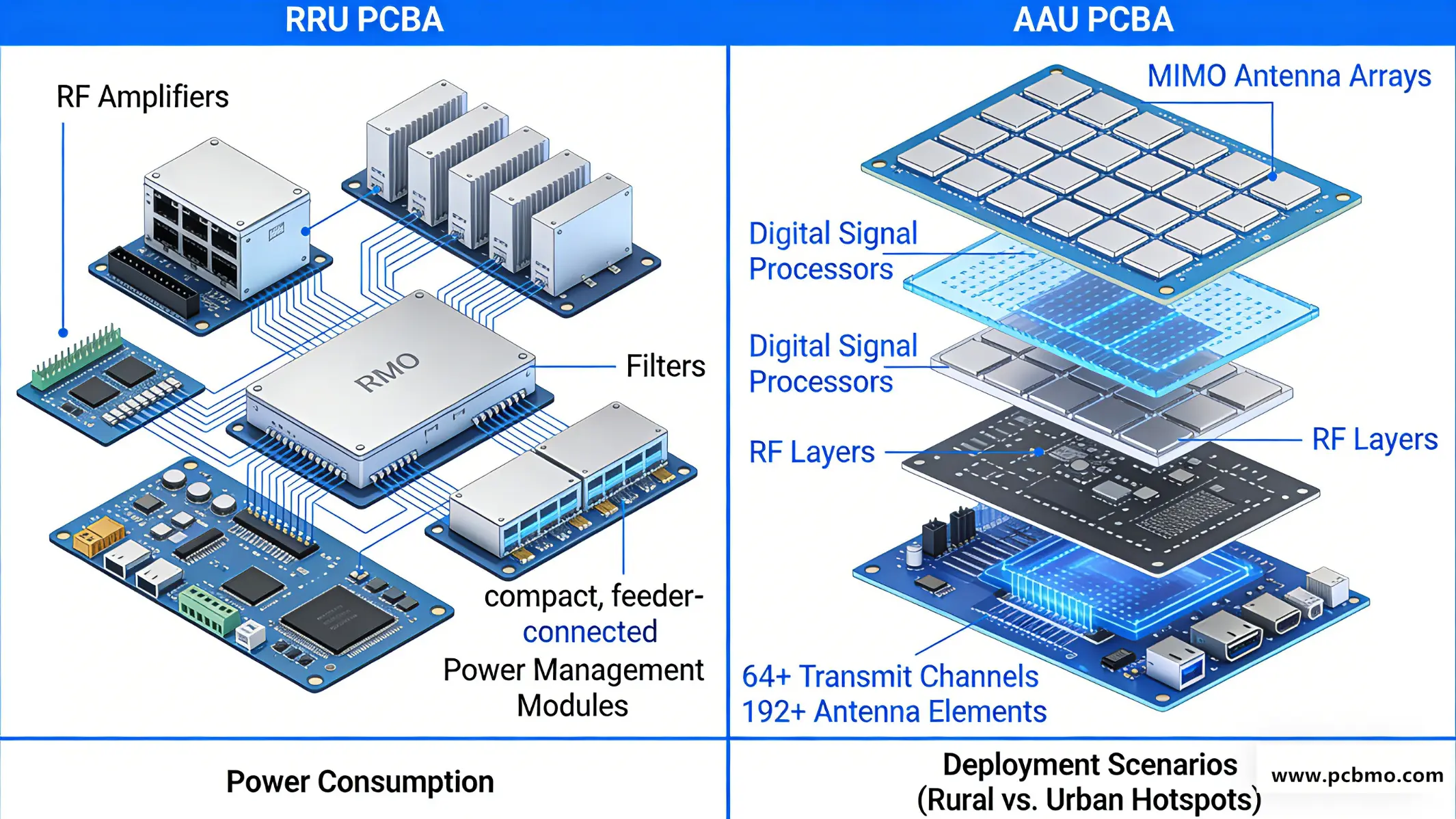
RRUs and AAUs serve distinct roles in wireless networks, with their PCBAs tailored to unique functional requirements. RRU PCBA focuses on radio frequency (RF) signal conversion and transmission, operating as a discrete unit connected to antennas via feeders. Its design prioritizes compactness and remote deployability, making it suitable for rural or low-capacity areas where cost and power efficiency are critical. Typical RRU PCBA integrates RF amplifiers, filters, and power management modules, supporting 2G/3G/4G multi-standard compatibility.
In contrast, AAU PCBA embodies high integration, merging RRU functionality with antenna arrays and digital signal processing units—an essential evolution for 5G Massive MIMO technology. 5G AAU PCBA must handle 64+ transmission channels and 192+ antenna elements, demanding dense interconnects and advanced thermal management. Deployed in urban hotspots and high-traffic zones, AAU PCBA delivers enhanced coverage and capacity, though at higher power consumption (up to 1150W per unit) compared to RRU counterparts.
Key Technical Requirements for Base Station & RRU/AAU PCBA
High-Frequency Signal Integrity
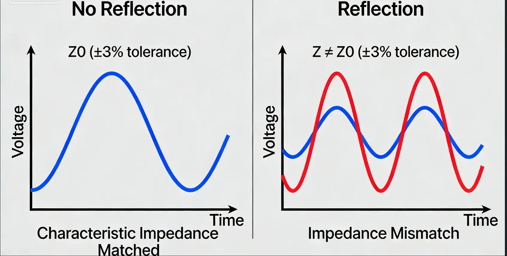
5G’s shift to Sub-6GHz and millimeter-wave bands exacerbates signal attenuation and skin effect losses, posing strict demands on RRU/AAU PCBA materials and layout. Conventional FR-4 laminates fail to meet high-frequency needs, so manufacturers adopt ultra-low-loss materials like Rogers RO4350B or ceramic-filled PTFE with dielectric loss (Df) ≤ 0.002 and stable dielectric constant (Dk) ± 0.05. Precision impedance control (±3% tolerance for 85Ω differential pairs) and laser-drilled microvias (≤0.1mm diameter) minimize signal reflection and discontinuity.
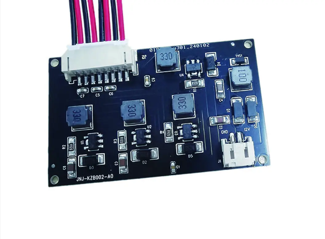
Thermal Management for High-Power Operations
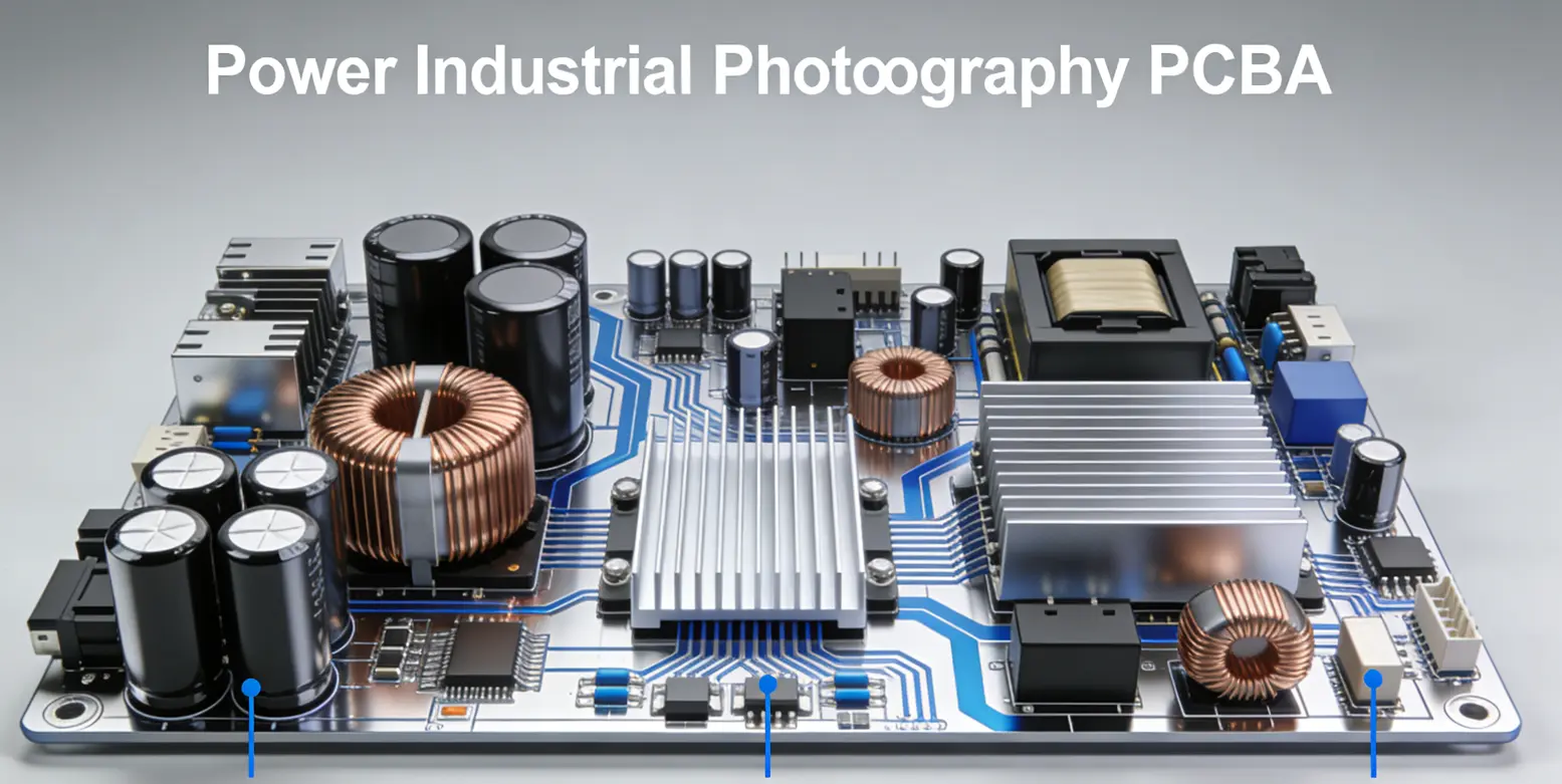
5G AAU PCBA dissipates 3–4 times more power than 4G equipment (up to 4000W per base station), requiring innovative cooling solutions. Embedded copper coins under RF amplifiers reduce thermal resistance by 60%, while aluminum nitride (AlN) ceramic patches integrated with FR-4 boost thermal conductivity to 5 W/(m·K). Thick copper layers (10 oz) and copper-based heat pipes further mitigate hotspots, ensuring PCBAs survive extreme thermal cycles (-40°C to 125°C).
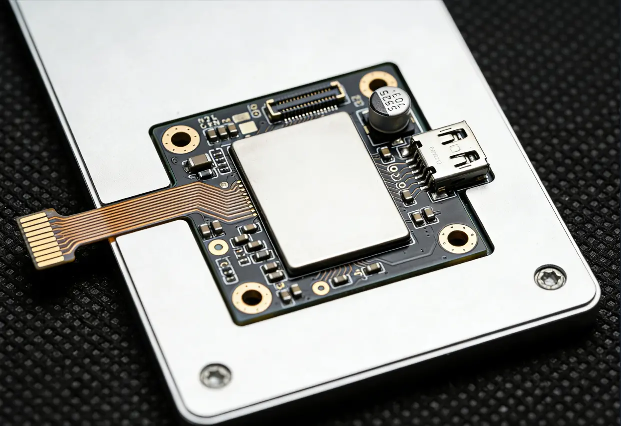
Density and Integration Capabilities
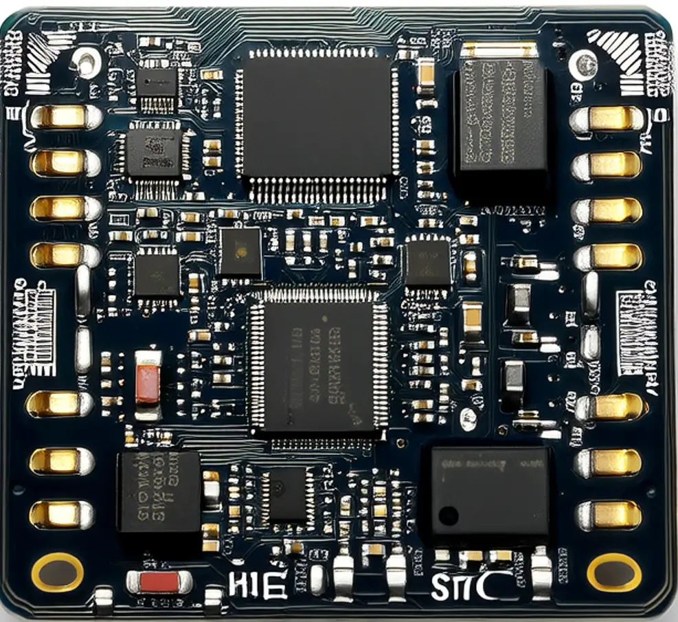
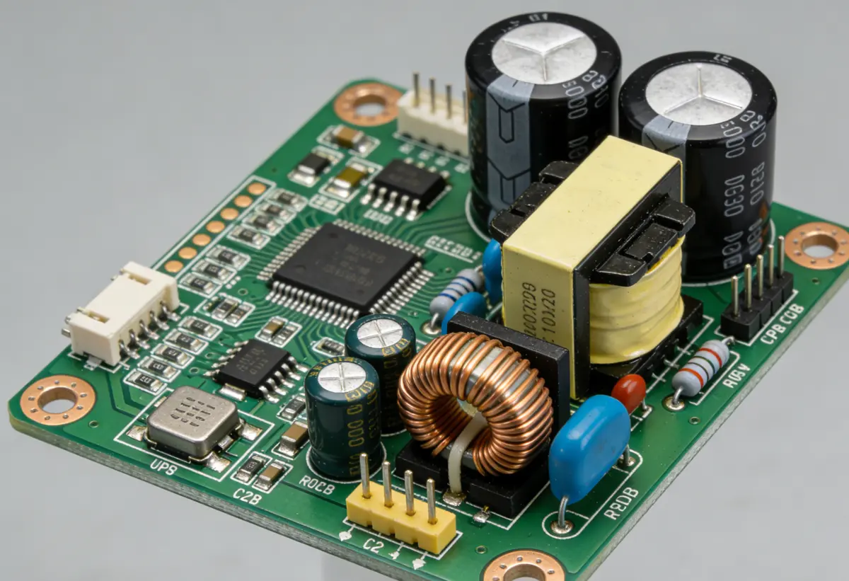
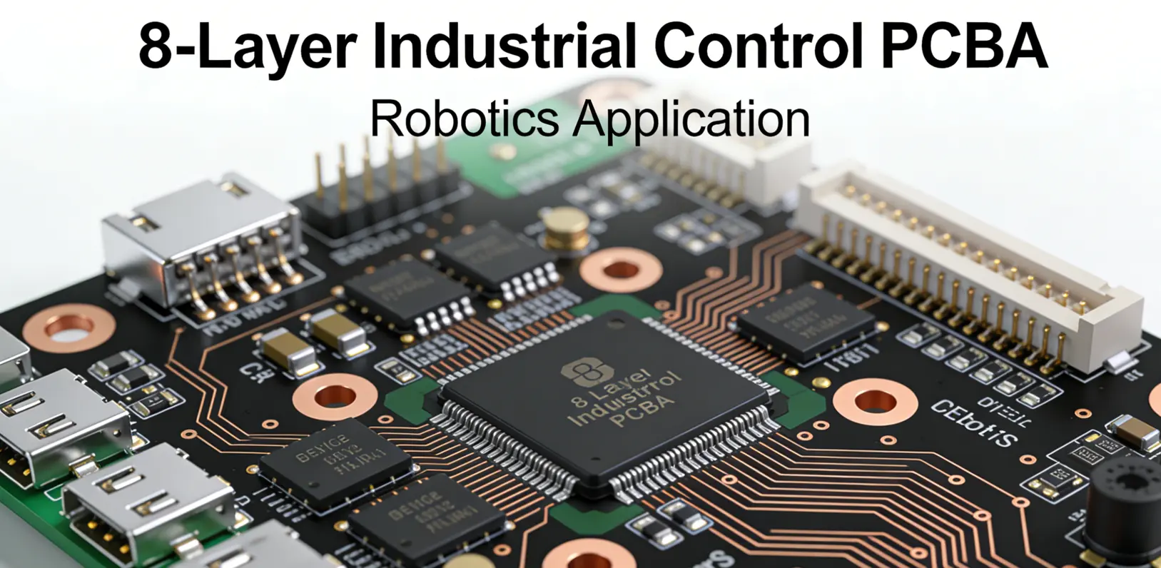
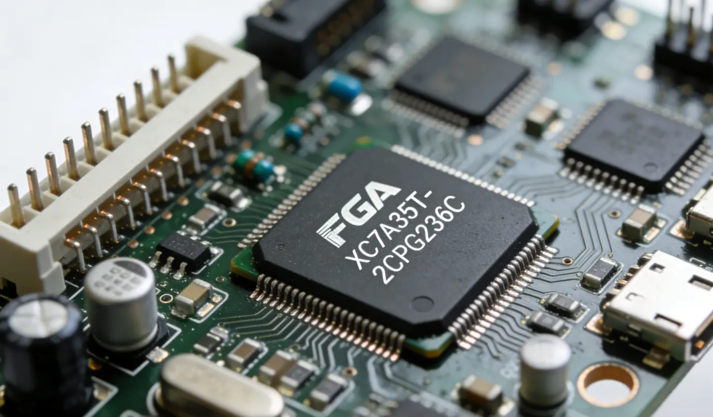
Massive MIMO technology drives the need for ultra-dense RRU/AAU PCBA designs. Any-layer HDI (High-Density Interconnect) structures with 2mil/2mil line/space enable routing for 0.4mm-pitch BGAs, while vacuum resin filling eliminates microvoids in microvias, enhancing reliability. AAU PCBA integrates not only RF components but also digital signal processors and power management units, requiring optimized component placement to balance performance and manufacturability.
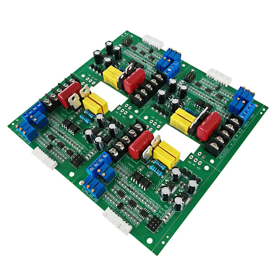
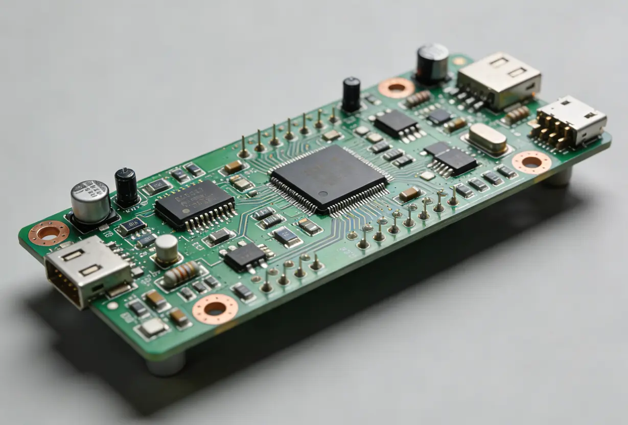
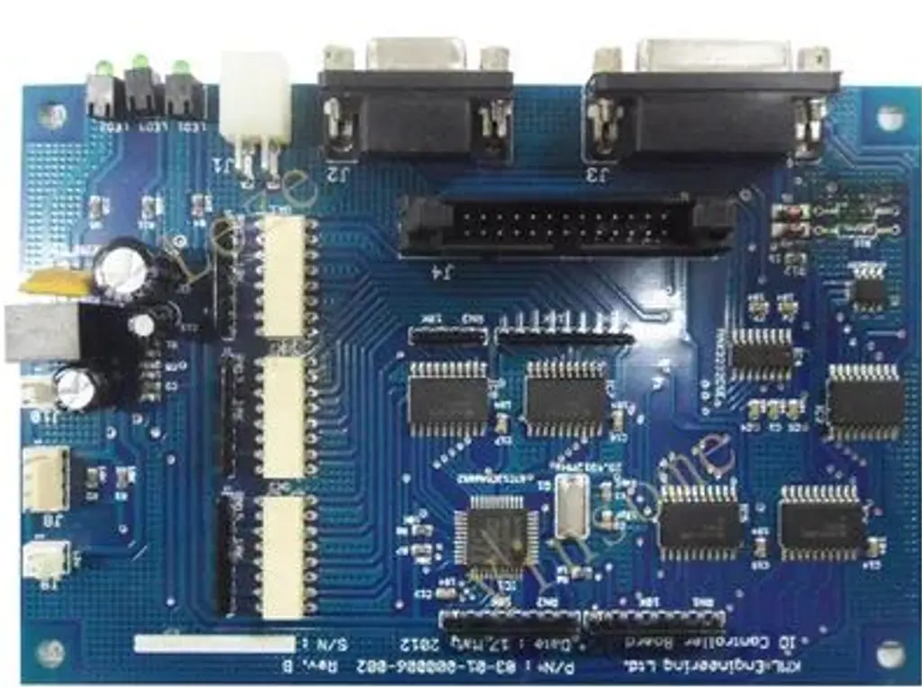
Manufacturing Processes for Reliable RRU/AAU PCBA
Base station & RRU/AAU PCBA manufacturing follows rigorous workflows to ensure durability in harsh outdoor environments. The process begins with precision layout design using specialized software, followed by material preparation with high-quality substrates like TU883. Chemical etching creates conductive pathways, and multi-layer bonding forms 10+ layer stackups. Surface treatment via immersion gold enhances corrosion resistance, while post-manufacturing testing—including TDR (Time Domain Reflectometry) and thermal cycling tests—validates signal integrity and reliability.
For 5G AAU PCBA, laser direct imaging (LDI) achieves ±0.076mm line-width accuracy for 40GHz antenna feeds, critical for Massive MIMO performance. Automated optical inspection (AOI) and X-ray inspection detect microdefects in dense interconnects, reducing failure rates in field deployments.
Future Trends Shaping Base Station & RRU/AAU PCBA
As 5G advances toward 6G, RRU/AAU PCBA technology will evolve to support higher frequencies, lower latency, and AI-driven optimization. Nanoparticle-reinforced laminates with dynamic Dk tuning are under development for 6G readiness, while hybrid stackups (PTFE for RF layers, FR-4 for digital sections) balance performance and cost. Additionally, energy-efficient designs—such as distributed power supplies and intelligent power management—will address AAU’s high power consumption challenge, aligning with global sustainability goals.
Edge computing integration with base station PCBA will further reduce latency, enabling applications like autonomous vehicles and industrial IoT. Modular RRU/AAU PCBA designs will also gain traction, allowing operators to upgrade components without full unit replacement, lowering lifecycle costs.
|
Parameter |
Technical Requirement |
|
Substrate Material |
High-frequency laminates: Rogers (4350B, 5880), Arlon AD1000, Isola FR408HR; FR-4 with high Tg (≥170°C) for low-loss signal transmission |
|
Dielectric Constant (Dk) |
2.2–3.5 (at 1–10 GHz) for high-frequency sections; 4.2–4.7 for low-frequency control circuits |
|
Dielectric Loss Tangent (Df) |
≤0.003 (at 1–10 GHz) to minimize signal attenuation |
|
Tg Value |
≥170°C (standard); ≥200°C (high-reliability applications) |
|
CTI (Comparative Tracking Index) |
≥600V (UL 746A) for anti-corrosion and insulation safety |
|
Copper Thickness |
1oz (35μm), 2oz (70μm), 4oz (140μm); ½oz (17.5μm) for fine-line high-frequency circuits |
|
Substrate Thickness |
0.4–2.0mm; tolerance: ±10% |
|
Parameter |
Technical Requirement |
|
Minimum Line Width/Spacing |
3mil/3mil (0.075mm/0.075mm) for high-frequency signal traces; 5mil/5mil (0.125mm/0.125mm) for power/control lines |
|
Minimum Via Size |
Microvia: 0.1mm (drill diameter); Blind/buried via: 0.2mm; through-hole via: 0.3–0.5mm |
|
Via Pitch |
≥0.3mm (microvia); ≥0.5mm (through-hole via) |
|
Impedance Control |
±5% tolerance for characteristic impedance (50Ω for RF signals, 100Ω for differential pairs, 75Ω for video/coaxial signals) |
|
Layer Count |
8–32 layers (typical for AAU PCBA); 4–16 layers (for RRU/base station control boards) |
|
Solder Mask |
Green/black matte solder mask; high-temperature resistant (up to 260°C for 10s reflow) |
|
Silkscreen |
White epoxy ink; resolution ≥0.15mm line width; legible component labels and polarity marks |
|
Parameter |
Technical Requirement |
|
Component Packaging Compatibility |
SMD: 01005, 0201, 0402, 0603, 0805, QFP, QFN, BGA, LGA, CSP; Through-hole: DIP, connector pins |
|
BGA Pitch |
0.4–1.0mm; ball size: 0.25–0.5mm |
|
Placement Accuracy |
±0.03mm (for components ≤0402); ±0.05mm (for components ≥0603); ±0.02mm (for BGA/QFN) |
|
Soldering Technology |
Lead-free reflow soldering (Sn-Ag-Cu, SAC305); selective wave soldering for through-hole components |
|
Solder Paste |
Type 4 (20–38μm particle size) for fine-pitch components; Type 3 (25–45μm) for standard components |
|
Reflow Temperature Profile |
Peak temperature: 245–255°C; dwell time at >220°C: 60–90s |
|
Parameter |
Technical Requirement |
|
Operating Frequency Range |
600MHz–6GHz (sub-6GHz 5G); 24–40GHz (mmWave 5G, AAU exclusive) |
|
Insertion Loss |
≤0.5dB (at 2GHz); ≤1.0dB (at 6GHz); ≤2.0dB (at 28GHz) for RF transmission paths |
|
Return Loss |
≥15dB (at 1–6GHz); ≥12dB (at 24–40GHz) |
|
Isolation Between RF Channels |
≥30dB (at 2–6GHz); ≥25dB (at 24–40GHz) |
|
Cross-Talk |
≤-40dB (adjacent signal traces at 1–6GHz) |
|
Parameter |
Technical Requirement |
|
Temperature Cycling Test |
-40°C to +85°C, 1000 cycles; no delamination, solder cracking, or performance degradation |
|
Humidity Test |
85°C/85% RH, 1000h; insulation resistance ≥10^9Ω; no corrosion or short circuits |
|
Vibration Test |
10–2000Hz, 10g acceleration, 2h per axis; no component detachment or solder joint failure |
|
Thermal Shock Test |
-55°C to +125°C, 500 cycles; ΔT = 180°C; no structural damage |
|
IP Rating |
IP65 (for outdoor RRU/AAU PCBA; dustproof and waterproof) |
|
Parameter |
Technical Requirement |
|
DC Resistance |
≤50mΩ for power traces (2oz copper, 100mm length) |
|
Current Carrying Capacity |
1oz copper: 2.5A/mm width; 2oz copper: 4.0A/mm width (at 25°C temperature rise) |
|
Insulation Resistance |
≥10^10Ω (at 500V DC) between adjacent traces |
|
Voltage Withstand Test |
1.5kV AC, 1min; no breakdown or leakage current >100μA |
|
Parameter |
Technical Requirement |
|
AOI (Automated Optical Inspection) |
100% coverage; detection accuracy for missing components, tombstoning, solder bridges: ≥99.9% |
|
X-Ray Inspection |
For BGA/QFN; void rate ≤5% per solder joint; no internal cracks |
|
Functional Test |
100% RF performance testing; power-on self-test (POST); signal transmission verification |
|
IPC Standards Compliance |
IPC-A-610 Class 3 (high-reliability electronics); IPC-6012/6012D for PCB qualification |